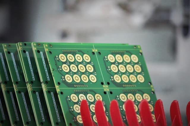
PCB Trace Technologies Inc makes various types of high-quality printed circuit boards for the electronics industry. These boards range from single-sided to double-sided and multi-layered. They also range from rigid boards to rigid-flex to flexible printed circuit boards. Our versatile boards are useful for a vast range of frequencies and are capable of handling very high frequency signals without loss of signal integrity.
We use various stack-ups for our multi-layered boards depending on their number of layers and their application. Stack-ups are the way we arrange different layers in a multi-layered board so that if operates in a definite manner when handling high frequencies, high voltage, or high current, etc. according to the application.
Multi-layered PCBs can have upward of 40 layers, and we must define these layers very carefully during the design phase. There are two ways we define the various layers in a PCB:
- Physical Layers
- Gerber Layers
The actual layers that make up the PCB are its physical layers. Each physical layer is made of a different material with its own functionality and purpose. On the other hand the Gerber film layers are the design layers to help the manufacturers fabricate the physical layers, and thereby the final PCB.

Physical Layers
Multi-layered boards are usually of balanced construction. That means, they have identical structures around the central layer. Although their structure and material may vary, the physical layers of a four-layer printed circuit board consists of several layers starting from the middle layer:
- Core
- Copper
- Pre-Preg
- Copper
- Solder Mask
- Surface finish
- Slikscreen
Typically, the manufacturer starts with a copper clad, a fiber-glass core with copper foil bonded on both sides. This forms the central core of the board. To build up the different layers, manufacturers mount multiple copper clads around the core. They insulate and separate the copper foils of adjacent copper clads with pre-preg material. Before mounting the various copper clads, they must drill and etch the copper foils to the required circuit for the layers. Each layer must match the registration marks on the preceding layer to build up the stack accurately.
Both pre-preg and core are important parts of a PCB. While the core provides the board with the required stiffness and thickness, the pre-preg is the insulating and bonding material between two copper foils. The pre-preg behaves as an adhesive material for the inner layers and as an insulating material for the inner conductive copper patterns.
During lamination, the fabricator squeezes the semi-cured epoxy in the pre-preg, causing it to flow and solidify. This bonds the multi-layer circuit boards together, thereby forming a reliable insulation.
A solder mask layer protects the outermost copper layers from oxidation, scratches, etc., but leaving out the copper pads that will undergo soldering. Surface finish protects the exposed solderable copper pads from tarnishing. A silkscreen layer provides information on positioning and orientation of various components on the board. It may also provide information on mounting various hardware.
The solder mask and silkscreen layers must be in contrasting colors to allow the information to be read easily.
Gerber Layers
To enable proper fabrication of each layer of a multi-layered board, designers must provide various information to the manufacturer. This information comes in the form of Gerber files and in different layers:
Mechanical Layers — Depending on the design of the PCB, the designer conveys the mechanical information of the board with Gerber files known as mechanical layers. These layers may provide the outer dimensions of the board, dimensions of the mounting holes if any, along with holes and cutouts for any component like connectors that require accurate positioning on the board.
Drilling Layer — The board may have through holes and the drill layers provides the X- and Y-coordinate information to the fabricator.
Routing Layers — These layers provide information about copper tracks and pads on individual layers including outermost layers. The fabricator uses this information to etch the copper foil on specific layers.
Copper Pour Layers — These layers provide information on ground planes and power planes in different copper layers. These planes connect to various onboard voltage points.
Split Plane Layers — Sometimes the ground planes or power planes may need splitting to enable them to connect to multiple voltage points. This layer offers the information about the split to the fabricator.
Keep-Out Layer — This layer provides crucial information about the separation of the copper features from the outer mechanical boundary of the board.
Solder Paste Layer — This layer provides information to the fabricator about the areas on the outermost layers of the board that will receive solder paste deposits. Usually, these will be the pads for mounting components. The information on this layer is also useful to a manufacturer making a stencil for the PCB. Accuracy is of importance here as the solder paste deposit must properly cover the pads.
Solder Mask Layer — This layer provides the fabricator with the information on the areas that the solder mask must cover.
Silkscreen Layer — This layer provides information on the text that appears on the outermost surfaces of the board. The text and lines on this layer identify various components, their location, and orientation on the board.
The fabricator uses the different Gerber layers as and when necessary. They can make films from the files and use photo-imaging techniques for transferring the information to the physical layer. Advanced PCB manufacturers like PCB Trace Technologies Inc use the Gerber layers to transfer the information directly to the physical layer.
Conclusion
PCB Trace Technologies Inc is an eminent PCB manufacturer in the US with over two decades of experience. We use the best technology to make printed circuit boards from top-quality copper clad laminate materials. We select the best FR-4 materials to make our boards. We ensure all PCBs we supply to our customers use qualified materials so that they experience the best printed circuit boards in the US.
