Check how easy it is to get a Full Trunkey quote in minutes

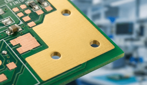
A common plating method, ENEPIG (Electroless Nickel Electroless Palladium Immersion Gold), is widely in use all over the world. Now, PCB manufacturers are also using the ENEPIG plating as it helps in bonding Gold wire balls. As the name suggests, the plating method uses a base layer plating of electroless Nickel, followed by a layer of electroless Palladium, and finally, a layer of Immersion Gold on top. Offering the optimum compromise between manufacturing ease and cost makes ENEPIG a very popular plating method.
ENEPIG plating is most suitable for bonding Gold wire balls, as the process increases the solderability of the PCB surface and produces excellent wire bonding. In the ENEPIG plating process, the thickness of the Nickel layer is typically 100-150 µin over the Copper layer, the thickness of the Palladium layer over the Nickel layer is 4-10 µin, and the topmost Gold layer is 1-2 µin thick.
Testing the PCB assembly is very simple. The testing method subjects a ball bump attached to the PCB surface to shear test. If the ball lifts off cleanly, or it peels off the Gold layer, exposing the layer of Palladium, then the plating has failed the test. The plating process can claim to have passed the test only when the ball leaves behind some residual Gold.
Another process, ENIG (Electroless Nickel Immersion Gold), is a plating process also offering a good ability of wetting and low cost. It also offers additional abilities like small form factor, finer tracks, finer pitch, and a high density of routing. Unfortunately, the ENIG process is also associated with the issue of black pads, making it incompatible with the process of bonding thermosonic Gold balls.
A PCB surface with electrolytic Nickel followed by electrolytic Gold on top also offers good wire bonding. However, the process has many disadvantages like high costs and the presence of large amounts of Gold makes solder joint reliability rather poor. Moreover, the process makes the co-planarity of the surface rather low and therefore, unsuitable for high density, fine pitch SMT components.
The ENEPIG surface plating method has none of the problems listed above. Adding the Palladium layer after the Nickel and before the Gold layer solves the issue of black pads, as it prevents hyper-corrosion of the Nickel while plating the Gold layer.
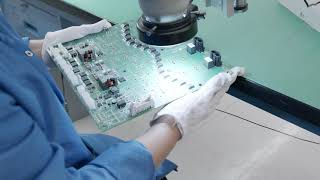
The standard process for bonding Gold balls requires a bond wire along with a stitch bond, and a ball bond. In general, such bonding increases the susceptibility of stitch bonds to be non-sticking compared to a surface with contamination and low plating quality.
As Gold is soft as a metal, a satisfactory wire bond requires an adequate Gold thickness. Inadequate Gold thickness may degrade the pull strength and result in a scraping of the underlying metal. A thick layer of Gold cushions the bond, making it stronger.


Increased Production Panel Output
We can now ship 100 production panels of 18"x24" in 5-7 working days for 2 to 10 layer designs.
A glimpse into PCB Trace