Check how easy it is to get a Full Trunkey quote in minutes

Traditionally, for bonding Gold ball wires manufacturers typically use a heavy layer of soft Gold on the surface of PCBs. The routine technique is to plate the copper tracks on the Printed Circuit Board with a Nickel layer, followed by an electroplated soft Gold layer, with a thickness of about 30-50 µm. When properly plated, the Gold layer forms a superior surface for bonding wires. Although expensive, the soft Gold plating method is adequately suitable for bonding fine-pitch Gold balls.
However, a reflow soldering process using Tin-based solder dissolves large amounts of Gold from the PCB surface, leading to extensive damage to patterns of Gold conduction. That makes solder joints brittle and increases the possibility to cracking due to fatigue. Therefore, rather than Tin-based solders, manufacturers prefer using Indium-based solders. As Gold does not dissolve in Indium, the results are more satisfactory.
Traditionally, wire bonding helps manufacturers in interconnecting chips to chip carriers, when they bond Gold wires to pads made of Copper or Aluminum. However, the bond reliability reduces due to the intermetallic migration of ions between Gold and Copper/Aluminum. Moreover, bonding between dissimilar metals reduces the robustness of the bond. The Copper/Aluminum surface usually has an oxide layer covering it, which the manufacturer must remove by plowing or scrubbing. Removing the oxide layer helps in improving the contact between the pad and the Gold wire, preventing potential pad damage.
When the Copper pad has an electroplated Nickel and Gold surface finish, Gold wire can bond easily with the Gold on the surface. As this bond does not create any intermetallic migration of ions, its reliability remains high. Moreover, the surface Gold does not oxidize, manufacturers do not need to scrub it, and this improves the quality of the bond. All the above allows use of smaller pads, leading to a reduction in chip sizes, while improving the IO count.
Surface finishing and electronic packaging industries regularly use the traditional electroplating process of Nickel and Gold. With Nickel acting as a barrier layer, the Gold layer forms a bonding surface. Manufacturers typically plate the layer of Nickel on the Copper pads before removing the photoresist and before etching. After they have etched the unwanted Copper and stripped the resist, the fabricator will usually apply a passivation layer of Polyimide. The passivation layer prevents the Copper sides below the Nickel from corroding. Finally, the manufacturer plates the layer of Immersion Gold on the Nickel layer, thereby creating a suitable surface on the top capable of wetting.
After completing the Nickel/Gold plating process, manufacturers bake the PCBs for an hour at 300°C. This allows the passivation layer to entirely cover the Copper sidewalls. Additionally, the baking process also allows the Nickel to diffuse into the Gold layer, hardening the Gold layer. However, this makes bonding wires more difficult. As this conventional approach to plating does not generate robust bonding pads, the process is also not suitable for bonding of Gold wires.
Therefore, PCB Trace Technologies Inc. uses a process of selective plating. We electroplate metals with TaTaN as the conducting layer. Our selective plating allows the electroplated Nickel layer and Gold to encapsulate the Copper layer entirely, thereby preventing corrosion of the Copper layer underneath.
In selecting the plating process, we first use sputtering to deposit a liner of TaTaN on the Copper layer. After this, we put photoresist on the Copper layer with the photolithography process. Then we remove unwanted Copper using the electro etching process. Once we have stripped the photoresist layer, we electroplate the Nickel and Gold layers on the Copper that we earlier lined with TaTaN.
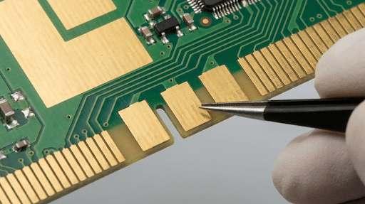
The Nickel layer has a thickness of about 1 µm, and the Gold layer is about 0.5 µm thick. This buries the Copper layer completely beneath the layers of Nickel and Gold.


Increased Production Panel Output
We can now ship 100 production panels of 18"x24" in 5-7 working days for 2 to 10 layer designs.
A glimpse into PCB Trace