Printed circuit boards (PCBs) — All modern electronic equipment use them. PCBs serve as the mechanical support for all components and provide the necessary circuitry to connect those components electrically to one another.
PCB Types
- Rigid PCBs — A vast majority of PCBs are made from a rigid substrate. The inflexible material provides a very stable and inexpensive support for component assembly. Rigid PCBs are available in single-sided, double-sided, and multilayer types.
- Flexible PCBs — also known as flex PCBs, these are made from flexible substrates. The flexibility of the board assembly allows it to bend and fit into tight or compact spaces. They are also available for dynamic flex applications, where the PCB can bend for hundreds of thousands of cycles without failure. Flexible PCBs are available in single-sided, double-sided, and multilayer types.
- Rigid-flex PCBs — are a hybrid of rigid and flex PCBs; they combine the advantages and eliminate the disadvantages of the other two PCB types by combining flexible circuits with rigid boards. The resulting design is a board assembly with the versatility of flexible PCBs and the strength and stability of rigid PCBs. Additionally, rigid-flex PCBs are suitable for use in much more mechanically challenging and complex electronic designs.
- HDI PCBs — Acronym for High-Density Interconnect PCBs. This is a type of PCB fabrication technology, using blind micro-via technology to manufacture PCBs with high trace density.

PCB Constituents
- Core or Base Material — The core or base material, also known as substrate, can be either rigid or flexible. Typical rigid materials include FR4, while typical flexible materials include high-temperature polyimide films, PEN plastic and polyester laminates. The substrate is an insulating base for the conductive circuits. Some boards use both rigid and flexible materials.
- FR4 — This is the most popular Fire-Retardant PCB substrate. This material consists of epoxy resin impregnated glass cloth. Manufacturers sometimes mix additives with the epoxy resin to further improve the material’s performance for more demanding applications. FR4 has good physical, mechanical, thermal, and electrical performance. It is also inexpensive. These factors make it suitable for use in a wide range of electronic applications.
- Prepreg — This is a dried and resin coated thin sheet of glass fabric. The glass core helps to stabilize the fabric. Under heat and pressure, the resin flows out and encapsulates the internal circuitry, forming the core of a rigid board.
- No-Flow Prepreg — This is a composite material requiring a longer period of resin curing, reducing the resin’s ability to flow under heat and pressure. No-flow prepregs are critical for rigid-flex designs, as they ensure the resin remains contained to the rigid portion of the board. Standard prepregs are not suitable for such hybrid PCB designs, as the regular resin flow could compromise the flexible portions of the rigid-flex PCB.
- Conductive Circuit Material — Most commonly used conductive circuit material is copper, chosen for its high electrical conductivity. At first, manufacturers laminate copper foil on to one or both sides of the substrate material. Then, PCB fabricators etch and remove extra copper from the circuit in accordance with the design specifications provided by the designer, to form conductive circuits or traces and pads. Multilayer PCBs consist of many layers of conductive circuit material. The number and thickness of conductive layers depend on the intended application.
- Via — This is a hole in a PCB board allowing for a conductive connection between layers. Vias may connect inner layers to one another and, in some cases, to outer layers. Blind vias connect inner layers to one of the external surfaces without penetrating the entire board. Buried vias only connect internal layers; they do not reach the outer layers. Through vias span the entire thickness of the board.
- Filled/Plugged Via — These are vias filled with an epoxy resin. Filled/Plugged vias prevent solder wicking.
- Tented Via — A via with a solder mask of dry film covering both its pad and its plated-thru barrel. The solder mask insulates the via totally, preventing solder wicking. Vias may be tented only on one side to allow attaching testing probes on the other.
- Via in Pad — A PTH positioned within a pad. Since a via in pad does not take up extra space on the PCB, It opens up more channels for routing, allowing very high density breakout of fine pitch components like BGAs. Via in pads are typically plugged and plated over to prevent solder wicking.
- PTH or Plated-Trough Hole — This is a through hole in a PCB with its hole walls plated. These holes are typically made for inserting a component. They facilitate insertion of either a component pin, termination, or wire for creating an electric connection from one side of the PCB to the other.
- NPTH or Non-Plated-Through Hole — This is a through hole in a PCB, but without any plating. Intended mainly for guiding or mounting mechanical components, no electrical connections are possible using this type of hole.
- Supported Holes — Another name for a PTH. A supported hole can support functions relating to thermal or electrical conductivity.
- Unsupported Holes — Holes with a pad on the solder side, but no pad on the component side. Unsupported holes do not have any plating inside them. These holes have no conductive function.
- Solder Mask/Solder Resist — A layer of thin insulating material called soldermask coats and protects the circuits on the surface layers or outer layers of the PCB. The coating protects these circuits from oxidation and prevents solder bridging during soldering of components on the PCB. Although green soldermask is the most common material, other colors are also available, such as clear, red, black, white, and blue.
- Surface Finish — The coating applied to exposed copper surfaces to protect them from oxidation and improve solderability (e.g., HASL, ENIG, OSP).
- Silkscreen/Nomenclature — Nomenclature, silkscreen, or legend refers to characters, mostly numbers and letters, printed on the soldermask. The characters provide identification and orientation for components and may include other important information. They help ensure proper assembly of components on the PCB.
- Electronic Components — Necessary to allow proper functioning of the assembled PCB. Electronic components are of two types. They may be of SMT or Surface Mount Technology type, attached to the surface of the board. They may also be of THT or Through-Hole Technology type, threaded through pre-drilled holes in the PCB.
- Conformal Coating — This is a continuous film coating for either protecting, insulating, or decorating the PCB.
PCB Design Terms
- Aspect Ratio — This is the ratio between the thickness of a PCB and the diameter of its smallest via. Keeping the aspect ratio low helps improve plating quality and minimizes potential via failures.
- Annular Ring — This term refers to the copper pad area left over after drilling a hole through it. To measure the width of the ring start from the pad edge and finish on the hole edge. The term annular ring is critically important to PCB design. It allows a proper electrical connection to be made from one side of the hole to the other.
- Single Board and Panel — A manufacturing method of the PCB in terms of its volume. Typically, it is usual to classify a board as one of two types: single unit or panel. In single unit manufacturing, the fabricator makes the PCBs one by one. In panel manufacturing, multiple units of PCBs are made in a single panel as an array.
- Array — This refers to a combination of multiple copies of the same PCB in a matrix. An array may also be referred to as a panelized, stepped out, or palletized PCB. Assembling boards in an array takes less time to complete.
- Controlled Impedance — The impedance of a circuit refers to a measure of its resistance and conductivity and is indicated in Ohms. Resistance is the opposition the circuit presents to current flow due to the inherent characteristics of the material. Controlling the impedance of a PCB trace to a specific value allows it to transfer high speed signals across the board without distortion, thereby improving the PCB functionality. This is essential in ensuring repeatable performance, especially in high-frequency and high-speed applications. It is essential to carefully match the substrate material and its electrical characteristics to the trace design and dimensions to ensure the electrical signal traversing the trace is always within a certain range of the expected value.
- PCB Stiffeners — These are mechanical support components for flex PCBs. They add rigidity to areas of the flex circuit that need it.
- Copper Weight — This term indicates the thickness of copper foil on each layer of a PCB. It is typically expressed in ounces per square foot.
- Countersink Holes — These are holes drilled into a PCB in the shape of a cone. They permit a countersunk screw to be flush with the PCB surface.
- Counterbored Holes — These are cylindrical holes drilled into a PCB to use with a fastener. They permit the fastener to be flush with the PCB surface.
- Mounting Holes — These are holes intended to secure a PCB to its final location in a device. To ensure no electrical interference, mounting holes are typically non-conductive and NPTH.
- Half-Cut/Castellated Holes — These are holes drilled on the edge of a board and plated, resulting in half-circle holes. PCBs designed for microchip testing typically use castellated holes.
- Slot Holes — Non-round holes on a PCB that may or may not be plated. Typically required for specific components, slot holes can increase the PCB cost due to the labor needed to cut them.
- Cutout — This is a small piece removed from a PCB.
- Daughter Board — A part separated from the main or mother board, a daughter board may contain plugs, sockets, pins and connectors.
- Bare Board — The term refers to a circuit board with no components mounted on it.
- Pad — A copper contact point on the PCB used for soldering component pins.
- Trace — A thin copper track interconnecting two pads or lands of copper.
- Trace Width — Width of a copper track or trace on a PCB.
- Spacing — Distance between neighboring traces on a PCB.
- Internal Layer — A term referring to the inner layers in a multi-layer PCB. Inner layers are mostly signal layers.
- External Layer — A term referring to an outer layer or exposed layer. Typically, components are mounted on the external layer.
- Layer-to-Layer Spacing — The distance between adjacent PCB layers. Thinner the spacing, more difficult the manufacturing process will be.
- Assembly — A process involving a series of procedures where components and accessories are placed on a PCB, prior to soldering them.
- Component Side — The side of the PCB containing components. For boards with surface mount components, this side is also the solder side. For boards with through hole components, however, the solder side is the side opposite to the component side.
- Connector — General term for a mechanical component interconnecting two or more PCBs or cables in an assembly. Typically, connectors consist of a plug and receptacle, which can be easily interconnected or separated.
- Edge Connector — A special type of connector designed for mounting on the edge of a PCB. Typically, used to facilitate an add-on card.
- Edge Plating — A term used for copper plating typically stretching from the top to the bottom of a surface and along the edges of a board. Edge plating allows for edge soldering and connections.
- Fingers — Metal pads along the edge of a board. Typically used for connecting two circuit boards together to expand their capacity.
- Gold Fingers — Connectors on the edge of a PCB after the board has been plated with gold. Hard, smooth and flat, these fingers are excellent conductors, supporting edge-to-edge connections.
PCB Fabrication Terms
- Fabrication Drawing — This drawing is a way for designers to communicate a PCB design to engineers and workers. It will typically include an illustration of the board, locations and information about holes to be drilled, notes about the materials and methods involved, etc.
- CAM Files — CAM is an acronym for computer-aided manufacturing, and the files produced by this software are used for PCB manufacturing. There are multiple types of CAM files, including Gerber files for photoplotters and NC Drill files for NC Drill machines. These files are usually sent off to board and assembly houses for refinement and eventual manufacturing.
- V-Scoring — An incomplete cut through a panel, typically helping in breaking apart panels of PCBs into single units.
- Etching — The process of removing unwanted copper from the PCB to create the desired circuit pattern.
- Gerber Files — Standard file format used to describe PCB design data, including copper layers, solder mask, and silkscreen information.
- Drill File — A file that specifies the locations and sizes of holes to be drilled in the PCB for component leads and vias.
- Surface Finish — The coating applied to exposed copper surfaces to protect them from oxidation and improve solderability (e.g., HASL, ENIG, OSP).
- Panelization — The process of grouping multiple PCBs onto a larger panel for improving fabrication efficiency.
PCB Assembly Terms
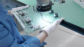
- Assembly House — A name used to refer to a manufacturing facility where PCBs and components are assembled. Such facilities usually contain PCBA equipment such as a screen printer, pick-and-place mounting machines, wave soldering machines, reflow ovens, and more.
- Assembly Drawing — An assembly drawing is a reference depicting the assembly requirements of a PCB. These drawings will typically include the placements of components as well as the construction technologies, methods and parameters needed to make it happen.
- Pick-and-Place Machine — An automated machine that picks up electronic components and places them onto the PCB according to the design specifications.
- Stencil — A thin metal or plastic sheet with openings used to deposit solder paste to specific areas of the PCB before component placement.
- Stencil Printer — A machine used to accurately apply solder paste to the PCB using a stencil.
- Solder Paste — A sticky, paste-like material containing solder particles applied to the PCB’s solder pads to facilitate component attachment during reflow soldering.
- Reflow Soldering — A process that melts solder paste to anchor components and create electrical connections between components and the PCB by passing it through a carefully controlled temperature profile.
- Reflow Oven — A specialized oven used for reflow soldering, with precise temperature control to ensure proper solder joint formation.
- Wave Soldering — A soldering method that passes the PCB over a wave of molten solder, which solders the through-hole components on the underside of the board.
Get a custom quote
Get an offline quote


Increased Production Panel Output
We can now ship 100 production panels of 18"x24" in 5-7 working days for 2 to 10 layer designs.
A glimpse into PCB Trace