Check how easy it is to get a Full Trunkey quote in minutes

HDI PCB Manufacturer
PCBs with High Density Interconnect technology are now commonplace in the miniature electronic products like tablets, wearables, and smart devices. PCB Trace Technologies Inc incorporates HDI technology in the basic PCB fabrication and the way the components connect to it.
However, limiting the HDI technology to just the interconnections between various printed circuit boards is not doing it justice. The technology involves special processes in the fabrication of the board itself, and to the connections between the SMT components present on its surface.
Fine Pitch Components
PCB miniaturization requires using surface mount technology components with fine pitch. Mounting these components is possible only with HDI technology, as they require:
- Densely packed traces and pads on a PCB
- Multiple layers on a single PCB
- Micro-vias for carrying signals between PCB layers
- Tight tolerances on PCB features
Apart from helping to reduce the size and weight of boards, HDI technology also provides a substantial increase in the density of surface mount components on the PCB. Additionally, mounting miniature integrated circuits like flip chips and BGAs is possible only using the HDI technology.
Design Advantages of HDI
With HDI technology reducing the size and weight of an assembly, designers can fit it into smaller spaces than they can with a board of a conventional design. The lower mass also reduces the chances of the assembly of damage from mechanical vibrations and shocks.
Considerations for HDI Assembly
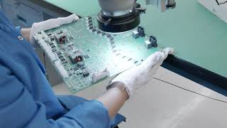
For an HDI PCB, placement of SMT components requires greater accuracy than for conventional PCBs, owing to much higher component density and finer pitch of the components.
For instance, Flip Chips and BGAs require special soldering techniques and additional process steps during assembly, rework, and repair.
HDI at PCB Trace Technologies Inc
If you require any assistance with HDI PCB design and assembly, our engineers are ready to help you. For more information on HDI PCB and assembly, simply contact us at 1 408-580-0722 or write to us at [email protected].
Frequently Asked Questions
1. What is HDI technology, and why is it important for modern electronics?
2. How does PCB Trace Technologies Inc. handle the manufacturing process of HDI PCBs?
3. What design advantages do your HDI PCBs offer to customers?
4. What are some assembly challenges of HDI PCBs, and how does PCB Trace Technologies Inc. address them?
5. Can PCB Trace Technologies Inc. assist with HDI PCB design and engineering support?
6. How can customers get started with HDI PCB services at PCB Trace Technologies Inc.?


Increased Production Panel Output
We can now ship 100 production panels of 18"x24" in 5-7 working days for 2 to 10 layer designs.
A glimpse into PCB Trace