Check how easy it is to get a Full Trunkey quote in minutes

HDI and Micro-Vias
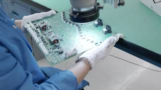
PCB fabricator must keep up with the steadily decreasing size of PCBs and their increasing complexities. Simultaneously, designers must constantly revise old processes, add new ones, and include those necessary for High Density Interconnect (HDI). As a PCB fabricator, PCB Trace Technologies Inc works constantly to stay on top of the game.
PCB Trace Technologies Inc specializes in HDI among other types of PCBs. However, it is not fine lines alone that makes an HDI board. These special boards require features like Sequential Build-Up (SBU) and laser-drilled Micro-Vias as well.
Sequential Build-Up
Sequential build-up for multi-layered boards requires adding one layer of dielectric or prepreg and a layer of copper foil at a time. The operator must etch and laser drill micro-vias on the copper foil before adding the next layer of dielectric and copper foil. The operator adds the layers to the substrates in pairs, each pair on either side of the substrate. This helps to balance the stress on the substrate. For instance, if the substrate is layer N and the layer pairs are 1, 2, and 3, the SBU arrangement will be 1+N+1, or 2+N+2, 3+N+3, and so on.
Laser-Drilled Micro-Vias
Being of very small diameter, laser-drilled micro-vias reduce the space required by traditional through-the-board vias. That means, circuit traces can have more space on the board.
A micro-via links only the layer of copper on which the operator creates it to the adjacent copper layer. That leaves the layers above and below the pair available for routing traces, which increases the overall circuit density tremendously.
With the addition of an SBU layer, the operator uses a laser beam to drill a hole from the outer copper layer through the dielectric directly below it to the inner copper layer immediately below. The operator then plates and fills all such holes in the copper layer. On adding another layer of SBU, the operator practically buries all the micro-vias they have just created.
Not all fabricators fill micro-vias. However, PCB Trace Technologies Inc. always fills all micro-vias with copper, as it makes the connections stronger and more reliable. The copper filling also helps with thermal management, improving the reliability of the entire board.
Fine-pitch SMT components frequently require via-in-pad or VIP to breakout the I/O lines. For VIPs, it is necessary to fill the micro-vias, not only to keep the pad smooth, but also to prevent the via from wicking molten solder away from the pad.
Filling the micro-vias has another advantage. It allows stacking of micro-vias one on top the other for connecting three or more copper layers, thereby increasing the circuit density further.
For more information on HDI technology and how it can help your project, contact PCB Trace Technologies Inc. over phone today, or write to us at [email protected].


Increased Production Panel Output
We can now ship 100 production panels of 18"x24" in 5-7 working days for 2 to 10 layer designs.
A glimpse into PCB Trace