HDI Technology in Hole
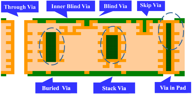
High Density Interconnection
 |  | 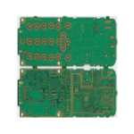 |  |  |  |
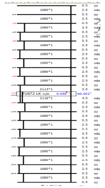
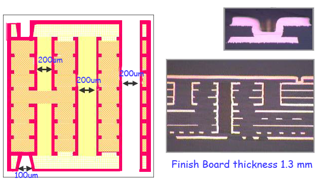
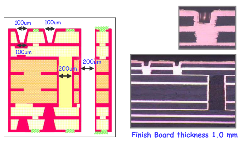
Blind & Burried 9+2+9 Laser Drill
 |  |  |
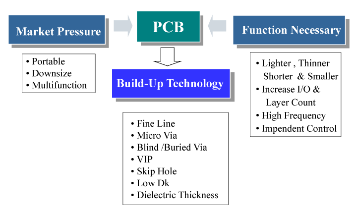
Market Trend vs. Technology Solution
HDI Process Flow
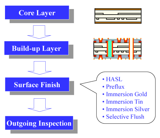
Main Process of Build – up Layer
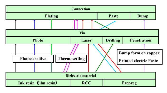
Construction Materials
MATERIAL TYPE
- FR 4 Tetra Function ( Tg. 130 – 140 ℃ )
- FR 4 High Tg ( Tg. 160 – 180 ℃ )
- RCC ( Tg. 150 ℃ & Tg. 185 ℃ )
- Ink ( VIL )
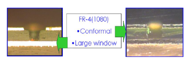
Comparison of Material
| Prepreg | RCC | |
| Low Cost | ++ | – |
| Strength | ++ | + |
| Hole wall roughness | – | + |
| Laminating control | + | – |
| Dielectric thickness | 45um ~ | 30um ~ 80um |
| Smear residue on target pad | – | ++ |
| Dielectric constant | 3.9 ~ 4.7 | 3.2 ~ 3.8 |
| Shelf time | ++ | + |
| Working PNL size | ++ | + |
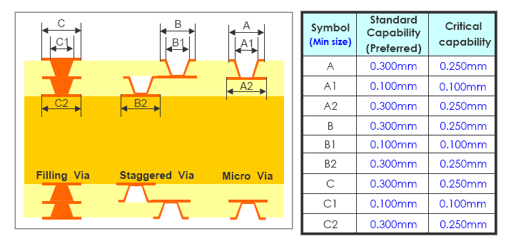
Comparison of Via Technologies
| Mechanical Drilling | Laser Drilling | |
| Low Cost in Equipment | ++ | + |
| Low Cost in Production | + | ++ |
| Required Facilities | Drilling Machine | Laser Machine |
| Consumable | Drill Bits, Backup Board | None |
| Aspect Ratio | 9 | 1 |
| Via Size Capacity | 200 um~ | 50~100um |
| Speed | 140 H/min | 20,000 H/min |
| Throughput | – | + |
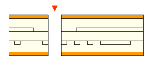
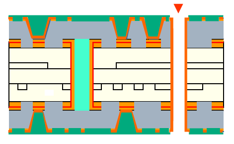
Comparison of Blind Via
| PREPREG | RCC |
 |  |
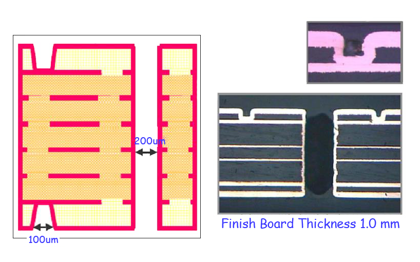
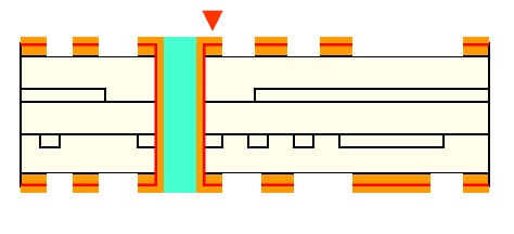
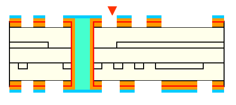
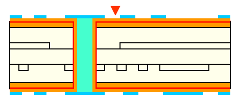
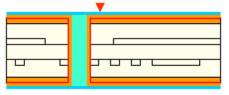
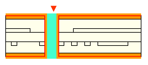
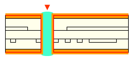
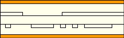
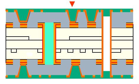
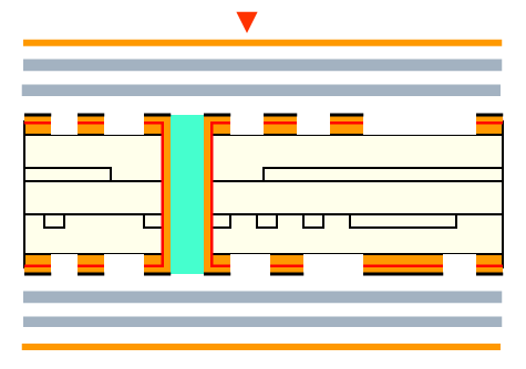
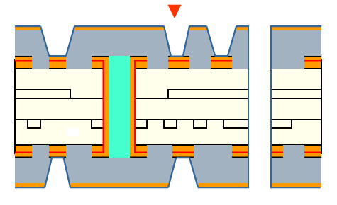
Build-up for 2 + N + 2
| THROUGH HOLE | INNER LASER VIA | STACK HOLE |
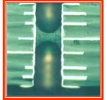 |  | 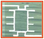 |
 |
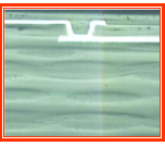
| INNER VIA HOLE | SURFACE LASER VIA |
 |  |
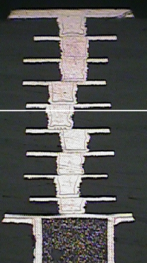
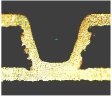
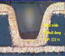
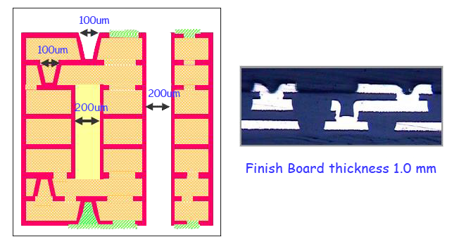
Laser Via Quality
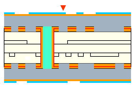
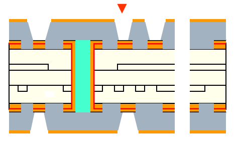
1+6+1 without buried, extend to 1+N+1
1+4+4+1 with buried via, extend to 1+N+N+1
Black Oxide Treatment
D.F. Strip
–
Etching
D.F. Exposure / Developing
Dry Film Lamination
I.V.H.Grinding( for thickness >= 60 mil )
I.V.H.Grinding( for thickness >= 60 mil )
Electro Plating

Electroless Copper Plating
I.V.H.(Inner Via Hole) Drilling
I.V.H.(Inner Via Hole) Drilling
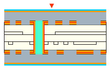
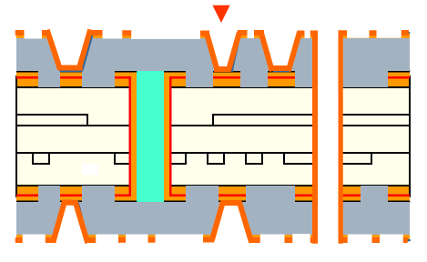
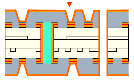
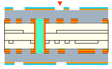
Blind via Capability
2+4+2 Staggered via, extend to 2+N+2
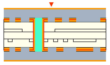
2+4+2 laser via on laser via
Solder Mask Printing
Dry Film Lamination
Lamination
Prepreg Layup
Black Oxide Treatment

D.F. Exposure / Developing
Dry film, Exposure & DES
Electro Plating
Desmear / Electroless Copper Plating

Laser Drilling for Blind Via
D.F. Strip

Etching
D.F. Exposure / Developing
–
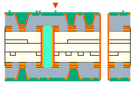
S/M Exposure / Developing
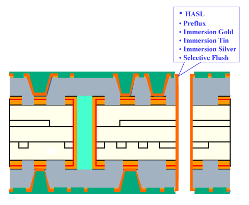
Surface Finish
Symbol Mask Printing
Inspection
–
Get a custom quote
Get an offline quote


Increased Production Panel Output
We can now ship 100 production panels of 18"x24" in 5-7 working days for 2 to 10 layer designs.
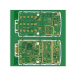
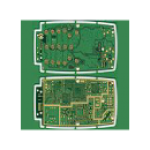
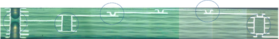
A glimpse into PCB Trace