As a leading printed circuit board designer in Silicon Valley, we at PCB Trace offer high-quality PCB layout and design services to our customers. We design all types of boards, and the capabilities we provide include:
PCB Layout and Design Services
- Single Layer
- Double Layer
- Multi-Layer
- Rigid Boards
- Flexible Boards
- Rigid-Flex Boards
- HDI boards
- Through-Hole Technology
- Surface Mount Technology
- Mixed Technology
We offer various techniques with our design services, including:
- DFM or Design for Manufacturing
- DFT or Design for Testability
- EMC or Design for Electromagnetic Compatibility
Contact us today for any type of design requirement. Our experienced engineers can help to bring your design to market in record time.
PCB Trace provides a highly experienced layout and design service. We also offer our customers various other services such as:

End-to-End Services
- Prototyping
- Electronic Design
- Software & Firmware Programming
- Optimized Software Architecture
- Testing & Certifications
- Security
- System Design
- Manufacturing & Quality Assurance
- Multimedia Applications
- Logistics
Free PCB Design
For first-time customers, PCB Trace is offering FREE PCB Design services. To avail of this offer, customers are requested to submit documents like:
- Schematic Drawing — in *.sch file / PDF file / Hand Drawn.
- Bill of Materials — In *.xlx / CSV / PDF / Text file / Print format
- Special Instructions for — Critical Component Placement, PCB Dimensions, Impedance Control, Speed and Frequency, Current and Voltage ratings, mounting arrangements, etc.
- Please ensure the PCB is a two or four-layer board and is smaller than 30 square inches in size.
- If your board has a complex design, please allow 5 to 7 days for design.
- We transfer all Gerber files to the customer as it is their property.
When developing your products, our experienced printed circuit board designers work closely with your electrical and mechanical engineers for ensuring the proper placement of parts. This ensures that your product meets the requirements of both the circuit and the mechanical architecture.
PCB Trace offers a wide range of PCB design services. These include schematic capture, Bill of Materials generation, PCB layout, board fabrication, component procurement, and PCB assembly. We have engineers with experience on various PCB CAD systems, while our primary tool is Cadence Allegro.
End-To-End Product Design and Development Services for PCB
PCB Trace also offers end-to-end product design and development services for printed circuit boards. We offer these services for an extensive range of products and IoT solutions.
Our end-to-end solutions include planning, design, product development, software services for numerous industries. We cover PCB design for industrial automation, building automation, healthcare services, manufacturing, commercial products, and several other businesses that need customized solutions.
Contact us today for all your PCB requirements.


Increased Production Panel Output
We can now ship 100 production panels of 18"x24" in 5-7 working days for 2 to 10 layer designs.
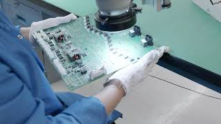
A glimpse into PCB Trace