Check how easy it is to get a Full Trunkey quote in minutes

A cost-effective and reliable flex circuit design depends on several factors, including:
- Capabilities and specifications of your flex design
- Proper material selection
- Requisite process tolerances
- Proper manufacturing logistics
- Experienced flex supplier
At PCB Trace Technologies Inc. our experts assist with your design aiming to reduce overall program cost. You can refer to our standard flex materials and capabilities. Should your design require special process treatments or tighter tolerances, please let us know.
Manufacturing Capabilities for Flex
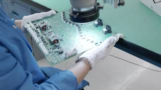
PCB Trace Technologies Inc. creates high quality bare flex boards, and this has been our major manufacturing capability for flex for the past few decades.
It does not matter whether if you need only a few custom PCB assembly boards done fast, require several boards for meeting your production schedule, boards with a single breakout, or highly complex RF/Microwave/Motherboard, PCB Trace Technologies Inc. will provide you with an efficient service.
Flex Capabilities
| Capability | Standard | Non-Standard |
| Layer Counts | 2-layers | 6-layers |
| Thickness (min) | 0.008” ±0.002” | 0.006” ±0.002” |
| Board Size | 7” x 13” | 7” x 21” |
| Trace / Space | 0.005” / 0.005” | 0.002” / 0.002” |
| Pad Size | 0.012” | 0.008” |
| Pad to Copper spacing | 0.005” | 0.004” |
| Hole Size (min) | 0.004” ±0.002” | 0.003” ±0.002” |
| Via Land | 0.005” | 0.004” |
| Hole to Board Edge | 0.015” | 0.010” |
| Dim (SM to SM) | 0.01” | 0.005” |
| SM to Copper | 0.015” | 0.005” |
| SM Color | Yellow | Yellow |
| Routing Tol | ±0.006” | ±0.002” |
| Finish | ENIG | ENIG |
Material selection, process tolerances, manufacturing logistics, and your flex supplier all play an important role in producing a cost-effective and reliable flex circuit design.
At PCB Trace, we will assist you in design for manufacturing to minimize overall program costs. Listed are standard materials and capabilities.
Come speak with us should your design require tighter tolerances or special process treatments.
Material Selection
| Polyimide Thickness | 0.0005″ (12 um), 0.001″ (25 um), 0.002″(50 um), 0.003″ (75 um), 0.005″ (125 um) |
| Copper (thickness) | 0.25 oz.(9 um), 0.33 oz.(12 um), 0.5 oz. (17 um), 1 oz.(35 um), 2 oz.(70 um) |
| Copper Foils(rolled-annealed) | Polyimide, Polyester, LPI (liquid photo imageable), PIC(photo imageable cover coat) |
| Stiffeners | FR-4, Polyimide, Metal, or customer supplied |
| Thermo-bond Adhesives | Acrylic, Phenolic Butyral, Modified Epoxy |
| Surface Finishes | Solder (hot air leveling or tin/lead plating), Electrolytic Soft Bondable Gold, Hard Gold, ENIG (electroless nickel immersion gold), Entek 106A, & Immersion Tin |
Process Capabilities and Tolerance
| Minimum Trace/Space | 0.0015″/.002″ (0.33 oz.) 0.002″/.0025″ (0.5 oz.) 0.003″/.0035″ (1 oz.) |
| Minimum Via Hole Diameter (before plating) | 0.006″ (NC Drill) 0.002″ (UV Laser) |
| Minimum Blind Via Diameter (before plating) | 0.004″ (UV Laser) |
| Trace to Edge Distance | 0.010″ ( NC Route ) 0.008″ (Die Punch) 0.001″ (UV Laser)* |
| Trace to Edge Tolerance | 0.005″ ( NC Route ) 0.003″ (Die Punch) 0.001″ (UV Laser) |
| Cover Layer Aperture Positional Tolerance | 0.005″ (Cover Film) 0.002″ (LPI and PIC) 0.001″ (Laser Ablation)** |
* Trace to edge distance should be greater than 0.003″ for proper copper insulation
** Laser defined apertures created by ablating cover layer material


Increased Production Panel Output
We can now ship 100 production panels of 18"x24" in 5-7 working days for 2 to 10 layer designs.
A glimpse into PCB Trace