Check how easy it is to get a Full Trunkey quote in minutes

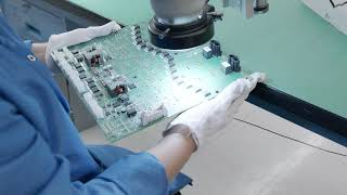
Ball-Grid Arrays (BGAs) are surface mount technology (SMT) devices with an array or pattern of solder balls on its bottom surface. The configuration of BGAs provides them with the flexibility necessary during temperature fluctuations, without causing stress to the solder connections between the balls of the IC and the PCB pads.
Mounting BGAs on the PCB requires the assembler to deposit solder paste on to the PCB pads using a stencil printing process. A pick and place machine then places the IC on to the PCB pads, with the solder balls under the BGA sitting directly on the solder paste deposits. The assembler passes the PCB assembly through the reflow oven to solder the BGA.
Ball Grid Array PCB Assembly
The primary advantage of the BGA package is that it can provide a substantially greater number of interconnections on a PCB than a conventional quad-flat IC pack can. Placing the BGA on the board requires precision to allow the balls to match with the pads on the PCB. The quantity of solder paste deposit on the PCB pads should be just enough to create a reliable junction.
BGA Advantages
As an SMT package, the BGA connects to pads only on the top surface of the PCB. Circuit traces from the pads route the connections to the rest of the circuit on the PCB. Efficient use of space on the board requires high density interconnections (HDI). As the IC pads directly connect to the pads, they offer very low inductance. Multiple connections allow better heat transfer away from the BGA.
BGAs are in great demand for several types of applications including data processing and storage, audio and video equipment, communication devices, medical and healthcare equipment, 3-D graphics systems, imaging, and radar and sonar equipment.
For any further information on Ball Grid Array technology, contact PCB Trace Technologies Inc at [email protected].


Increased Production Panel Output
We can now ship 100 production panels of 18"x24" in 5-7 working days for 2 to 10 layer designs.
A glimpse into PCB Trace