With the continuous miniaturization of electronic devices and increasing demand for high-density interconnections, traditional mechanical drilling methods have reached their physical and technical limits. Modern Printed Circuit Board (PCB) designs—especially High Density Interconnect (HDI) PCBs—require extremely small, precise, and reliable vias that cannot be achieved efficiently using mechanical drilling alone. Which can only be done with Laser dill production in PCBs.
Laser drilling has therefore become an essential process in PCB production for companies like PCB Trace Technologies Inc. It enables the creation of microvias with diameters as small as 50–75 µm, supporting advanced multilayer structures, fine-pitch components, and high-speed signal integrity.
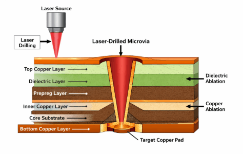
Overview of Laser Drill Production in PCB Manufacturing – A Quick Rundown!
Laser drilling is a non-contact material removal process that uses a highly focused laser beam to ablate dielectric material and create vias. Unlike mechanical drilling, laser drilling does not rely on physical tools, eliminating issues such as tool wear, drill breakage, and mechanical stress on thin PCB layers.
Types of Lasers Used in PCB Drilling:
- CO₂ Lasers (10.6 µm wavelength) are primarily used for drilling organic dielectric materials such as FR-4 and prepreg.
- UV Lasers (355 nm wavelength) provide high precision and are capable of drilling both dielectric and thin copper layers.
Dual-laser systems are commonly used, combining CO₂ and UV lasers for optimal drilling quality.
Applications of Laser Drilling in PCB Production
Laser drilling is widely used for microvias, via-in-pad structures, HDI PCBs, sequential build-up layers, and advanced packaging substrates.
Design Requirements for Laser Drilling
Proper PCB design is critical for achieving reliable laser-drilled vias.
1. Via Diameter and Aspect Ratio
Laser drilling is primarily used for creating microvias with small diameters, typically ranging from 50 µm to 150 µm. To ensure complete dielectric removal and uniform copper plating, the aspect ratio (via depth to via diameter) should be limited to 1:1 or less. Shallow vias allow the laser beam to efficiently ablate dielectric material and expose the target copper pad without causing excessive thermal damage.
2. Capture Pad and Target Pad Design
The capture pad on the build-up layer and the target pad on the underlying copper layer must be carefully designed to accommodate laser registration tolerances. The target pad diameter is generally designed to be 1.5 to 2 times larger than the microvia diameter. This ensures proper copper exposure at the via bottom, even with minor positional deviations during laser drilling.
3. Copper Thickness Requirements
Laser drilling performs best when copper thickness is tightly controlled. Thin copper foils, typically ≤18 µm, are preferred for build-up layers because they allow faster laser penetration and reduce the need for excessive laser energy. Thicker copper layers may require additional UV laser cleaning to remove residual copper at the via bottom.
4. Dielectric Thickness Control
Uniform dielectric thickness is critical for consistent laser drilling performance. Variations in dielectric thickness can result in under-drilled or over-drilled vias. For reliable microvia formation, the dielectric layer thickness is usually kept within 50–100 µm, depending on via diameter and laser capability.
5. Layer Stack-Up Considerations
Laser drilling is performed after lamination of the build-up layers in sequential lamination processes. The PCB stack-up must be designed so that laser-drilled microvias connect only adjacent layers. Skipped-layer microvias are generally avoided due to depth limitations and reliability concerns.
6. Registration and Fiducial Design
Accurate laser drilling requires precise alignment between layers. Global and local fiducials must be included in the PCB design to support optical alignment systems used in laser drilling machines. Proper fiducial placement improves drilling accuracy and minimizes via-to-pad misregistration.
7. Via-in-Pad Design Considerations
For high-density designs, laser drilling is commonly used in via-in-pad structures. In such cases, the via must be completely filled and planarized after plating to prevent solder voids and ensure reliable component assembly. Design rules must account for via fill material compatibility and surface finish requirements.
Material Requirements for Laser Drilling
Material selection significantly affects laser drilling quality and consistency.
1. Dielectric Materials
- Dielectrics must have consistent resin content and predictable ablation characteristics.
- Common materials include FR-4 (laser grades), RCC, and modified epoxy systems.
2. Copper Thickness
Laser drilling performs best when copper thickness is tightly controlled. Thin copper foils, typically ≤18 µm, are preferred for build-up layers because they allow faster laser penetration and reduce the need for excessive laser energy. Thicker copper layers may require additional UV laser cleaning to remove residual copper at the via bottom.
Equipment Requirements
Laser drilling machines must meet stringent performance requirements.
1. Laser Power and Pulse Control
Adjustable laser pulse energy and pulse frequency are essential for achieving consistent and repeatable microvia formation in PCB laser drilling. By precisely controlling the amount of energy delivered in each pulse and the number of pulses applied per unit time, the laser system can effectively ablate dielectric material without damaging surrounding copper features.
Short pulse durations are particularly important, as they confine thermal energy to a very small area and time interval, thereby significantly reducing the heat-affected zone (HAZ). This minimizes defects such as resin carbonization, glass fiber protrusion, and copper pad deformation.
Proper laser power and pulse control ensure uniform via depth, stable via diameter, and smooth via walls, which are critical for reliable copper plating and long-term electrical performance in high-density PCB applications.
2. Positioning and Registration Accuracy
Accurate positioning and registration are critical requirements in laser drilling, as microvias must be precisely aligned with underlying target pads to ensure reliable electrical interconnections. High-precision vision systems, typically based on CCD or CMOS cameras, are integrated into laser drilling equipment to detect global and local fiducials on the PCB surface.
These vision systems enable real-time alignment correction by compensating for panel shrinkage, distortion, and lamination-induced misregistration. Modern laser drilling machines are capable of achieving registration accuracy of ±10 µm or better, which is essential for fine-pitch HDI designs and via-in-pad structures.
Precise positioning prevents defects such as off-center vias, pad breakout, and incomplete copper exposure, thereby improving plating reliability, yield, and overall PCB performance.
3. Automation and Throughput
Automation and high throughput are essential requirements for laser drilling equipment in modern PCB manufacturing environments, where large panel volumes and tight production schedules are common. Advanced laser drilling systems support automated panel loading and unloading, reducing manual handling, minimizing human error, and improving process consistency.
In addition, recipe-based process control allows predefined drilling parameters—such as laser power, pulse frequency, focus position, and drilling sequence—to be automatically selected based on PCB design and material type. This enables rapid changeover between different products while maintaining consistent drilling quality.
High levels of automation, combined with optimized drilling speed and minimal downtime, significantly enhance production efficiency, yield, and cost-effectiveness in high-volume HDI PCB fabrication.
Process Control Requirements
Strict process control is necessary in laser drilling to maintain consistent drilling quality, high production yield, and long-term reliability of microvias. Laser drilling involves precise interaction between laser energy and PCB materials, making the process highly sensitive to parameter variations.
Without effective control, variations in via depth, diameter, and taper can occur across the panel, leading to defects in subsequent processes such as plating and via filling. Therefore, modern laser drilling systems rely on recipe-based control, real-time monitoring, and statistical process control (SPC) to ensure stable and repeatable drilling performance throughout mass production.
1. Laser Parameter Optimization
Optimization of laser parameters is critical for achieving defect-free microvias. Key parameters include pulse energy, repetition rate, focus position, and pulse count, all of which must be carefully matched to the dielectric thickness, copper weight, and via size. Proper optimization ensures complete dielectric ablation while cleanly exposing the target copper pad.
Improper parameter settings can result in defects such as resin smear, excessive overburn, glass fiber protrusion, or incomplete drilling, which negatively affect plating adhesion and electrical reliability. Consistent parameter optimization is therefore essential for maintaining uniform via geometry and process stability.
2. Debris Removal and Via Cleaning
Laser drill production generates ablation debris, carbonized resin, and glass fiber residues that can remain on via walls and at the via bottom. To remove these contaminants, plasma desmear or chemical cleaning processes are commonly applied after laser drilling.
Effective debris removal ensures clean via surfaces and fully exposed copper pads, which are critical for reliable copper electroplating and strong interlayer connections. Inadequate cleaning can lead to poor copper adhesion, voids, and early via failure, making thorough via cleaning an essential part of overall laser drilling process control.
Quality and Reliability Requirements
Laser drill production must meet strict quality and reliability requirements to ensure dependable electrical interconnections throughout the service life of the PCB. Because microvias are often used in high-density and high-speed circuits, even minor defects can lead to increased electrical resistance, intermittent connections, or early failure.
Consistent via quality is therefore essential not only for successful copper plating and via filling, but also for long-term thermal and mechanical reliability. Maintaining tight quality control during laser drilling directly contributes to higher yield, improved performance, and compliance with customer and industry requirements.
1. Via Geometry and Surface Quality
The geometry and surface condition of laser-drilled vias are critical indicators of drilling quality. The via bottom must be clean and fully expose the target copper pad, ensuring good electrical contact and strong copper-to-copper bonding during electroplating.
The via walls should be smooth and uniform with minimal taper, allowing for even copper deposition and reducing the risk of voids or thin plating areas. Excessive taper, resin residue, or surface roughness can compromise plating integrity and negatively impact the reliability of the interconnection.
2. Inspection and Testing
To verify the quality of laser-drilled vias, multiple inspection and testing methods are employed throughout PCB manufacturing. Optical microscopy is used for routine inspection of via alignment and surface cleanliness, while cross-section analysis provides detailed evaluation of via depth, wall profile, copper exposure, and plating thickness.
In addition, electrical testing is performed to confirm continuity and low resistance of interlayer connections. These inspection techniques help detect defects early, preventing yield loss and ensuring consistent product quality.
3. Industry Standards
Laser drilling processes and resulting microvia quality must comply with recognized industry standards to ensure reliability and interchangeability. IPC-2226 provides design guidelines for HDI PCBs, including microvia structures and stack-up requirements.
IPC-6012 and IPC-6016 define qualification and performance standards for rigid and HDI printed boards, specifying acceptance criteria for via quality, plating integrity, and reliability. Adherence to these standards ensures that laser-drilled vias meet established industry benchmarks and customer expectations.
Advantages of Laser Drill Production over Mechanical Drilling
Laser drilling offers significant advantages over conventional mechanical drilling, particularly for high-density and advanced PCB designs. It enables the formation of extremely small via sizes, typically below 150 µm, which are difficult or impossible to achieve using mechanical drills. Because laser drilling is a non-contact process, it eliminates mechanical stress on thin build-up layers, reducing the risk of delamination, cracking, and drill bit wear.
In addition, laser systems provide higher positional accuracy and better registration control, allowing precise alignment of microvias with underlying target pads. These benefits result in improved drilling consistency, higher production yield, and enhanced reliability, making laser drilling the preferred technology for HDI PCBs, via-in-pad structures, and miniaturized electronic products.
Challenges and Limitations of Laser Drill Production
Despite its many advantages, laser drill production also presents certain challenges and limitations in PCB manufacturing. Laser drilling equipment involves high initial investment and maintenance costs, making it less economical for low-volume production or simple PCB designs. In addition, the process requires careful and precise control of laser parameters, as improper settings can lead to defects such as resin smear, overburn, or incomplete via formation.
Laser drilling is also generally slower and less efficient for large through-hole vias compared to mechanical drilling, particularly when drilling thick boards. As a result, many PCB manufacturers adopt a hybrid approach, using laser drilling for microvias and mechanical drilling for larger through-holes to achieve optimal cost, speed, and reliability.
Conclusion
Laser drill production has become a critical technology in modern PCB production, driven by the increasing demand for miniaturization, higher circuit density, and improved electrical performance. Its ability to create precise and reliable microvias enables advanced HDI designs that are not achievable using conventional mechanical drilling methods.
However, the successful implementation of laser drilling, as mastered by PCB Trace Technologies Inc, depends on a combination of proper PCB design, suitable materials, advanced laser drilling equipment, and strict process control.
When these factors are carefully optimized and aligned, laser drilling delivers high-quality interconnections, improved manufacturing yield, and long-term reliability, making it an indispensable process in today’s PCB manufacturing industry.
