Reflow soldering is the primary soldering method used in Surface Mount Technology (SMT) assembly, where solder paste deposits printed on PCB pads are melted to form permanent electrical and mechanical connections. Proper thermal profiling is critical for solder joint reliability, component integrity, and long-term PCBA performance. At PCB Trace Technologies Inc, we prioritize this process to ensure the highest quality.
Fundamentals of Reflow Soldering
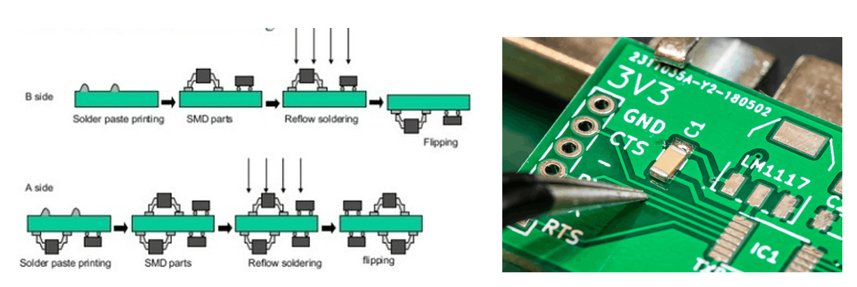
Reflow soldering is a controlled thermal process used to form reliable electrical and mechanical connections between surface-mount components and PCB pads. In this process, solder paste is first deposited onto pads, components are placed, and the entire assembly is heated in a precisely controlled environment.
As the temperature rises, the solder paste transitions from a solid to a liquid state, allowing the molten solder to wet the component leads and pads. Upon cooling, the solder solidifies to form strong and reliable solder joints. The success of reflow soldering depends on accurate thermal profiling and compatibility between materials, components, and equipment.
Reflow Soldering Equipment
Modern reflow soldering relies on specialized equipment designed to deliver uniform and repeatable heating across complex PCB assemblies. The most commonly used systems are convection reflow ovens and vapor phase reflow systems, each offering specific advantages depending on application requirements, board complexity, and thermal sensitivity.
1- Convection Reflow Ovens
Convection reflow ovens use forced hot air circulation to transfer heat uniformly to the PCB assembly. These ovens typically consist of multiple independently controlled heating zones, including top and bottom heaters, followed by dedicated cooling zones.
The multi-zone design allows precise control of ramp rates, soak duration, peak temperature, and cooling profiles. Advanced systems may include nitrogen capability to reduce oxidation and improve solder joint quality. Convection ovens are widely used in high-volume SMT production due to their flexibility, repeatability, and compatibility with lead-free soldering.
2- Vapor Phase Reflow (VPR)
Vapor phase reflow uses a saturated vapor of a heat-transfer fluid to heat PCB assemblies. Heat is transferred through condensation at a fixed boiling temperature, ensuring excellent thermal uniformity across the board. Because the temperature cannot exceed the boiling point of the vapor, the risk of overheating components is minimized.
Vapor phase reflow is particularly beneficial for assemblies with high thermal mass variation, dense layouts, or temperature-sensitive components, though it is generally used for specialized or low-to-medium volume applications.
Reflow Soldering Profile Overview
A reflow soldering profile is a time–temperature curve that defines how a PCB assembly is heated and cooled during the reflow process. The profile is divided into distinct stages—preheat, soak, reflow (peak), and cooling—each serving a specific purpose in flux activation, solder melting, and joint formation.
A properly PCB design profile ensures uniform heating, minimizes thermal stress, and produces reliable solder joints across all components.
Preheat Stage
The preheat stage is the initial phase of the reflow process, during which the PCB assembly temperature is gradually increased from ambient conditions.
– Purpose of Preheat
The primary purpose of preheat is to gently warm the PCB and components to prevent thermal shock. This stage activates the flux within the solder paste, allowing it to remove surface oxides, while also evaporating volatile solvents. Controlled preheating ensures a smooth temperature transition and prepares the assembly for uniform solder melting in later stages.
– Typical Parameters
During preheat, the temperature typically rises from room temperature to approximately 150 °C, with a controlled ramp rate of 1–3 °C per second. Maintaining a stable ramp rate helps prevent component cracking, PCB warpage, and solder paste spattering.
Soak (Thermal Equilibrium) Stage
The soak stage, also known as the thermal equilibrium stage, follows preheat and stabilizes the assembly temperature.
Purpose of Soak
The soak stage allows temperatures to equalize across components with different thermal masses, ensuring uniform heating before solder reflow. It also provides sufficient time for full flux activation and continued oxide removal, which is critical for proper solder wetting.
Typical Parameters
Typical soak temperatures range from 150–180 °C, with a duration of 60–120 seconds. Excessive soak time should be avoided, as it may degrade flux activity or oxidize component leads.
Reflow (Peak) Stage
Typical soak temperatures range from 150–180 °C, with a duration of 60–120 seconds. Excessive soak time should be avoided, as it may degrade flux activity or oxidize component leads.
Time Above Liquidus (TAL)
Time Above Liquidus (TAL) refers to the duration during which solder temperature remains above its melting point. For SAC305 lead-free solder, TAL typically ranges from 30–90 seconds, ensuring complete solder melting, wetting, and intermetallic formation without excessive thermal exposure.
Peak Temperature Control
Peak temperature must be high enough to achieve proper solder wetting but low enough to avoid component damage. For lead-free assemblies, peak temperatures generally range from 235–250 °C. Precise control of peak temperature is essential to prevent defects such as voiding, solder balling, or component delamination.
Cooling Stage
After reflow, the assembly enters the cooling stage, where molten solder solidifies to form final joints.
Purpose of Controlled Cooling
Controlled cooling determines the final solder joint microstructure, which directly affects mechanical strength and long-term reliability. Gradual cooling minimizes thermal stress and prevents cracking or brittle intermetallic formation.
Typical Cooling Rates
Recommended cooling rates range from 2–4 °C per second. Cooling too quickly may induce stress, while excessively slow cooling can weaken solder joint structure.
Lead-Free vs Leaded Reflow Profiles
Lead-free reflow profiles require higher peak temperatures and tighter thermal control compared to traditional leaded profiles due to the higher melting point of lead-free alloys. This increases thermal stress on components and PCBs, making accurate profiling, material selection, and process control even more critical in lead-free assembly environments.
| Parameter | Leaded Solder (Sn-Pb) | Lead-Free Solder (e.g., SAC305) | Notes / Implications |
|---|---|---|---|
| Melting Point | ~183 °C | ~217–221 °C | Lead-free requires higher peak temperature to achieve complete melting. |
| Peak Temperature | 215–225 °C | 235–250 °C | Higher peak for lead-free increases thermal stress on components and PCB. |
| Time Above Liquidus (TAL) | 30–60 seconds | 30–90 seconds | Lead-free TAL must be carefully controlled to ensure proper wetting and avoid damage. |
| Ramp Rate (Preheat) | 1–3 °C/sec | 1–3 °C/sec | Similar, but preheat is critical for lead-free to reduce thermal shock. |
| Soak Stage Temperature | 150–180 °C | 150–180 °C | Lead-free requires stable soak for uniform heating due to higher melting alloys. |
| Cooling Rate | 2–4 °C/sec | 2–4 °C/sec | Controlled cooling needed to avoid solder joint stress and cracking. |
| Flux Activity Requirements | Standard fluxes | Higher activity fluxes may be needed | Lead-free alloys oxidize more easily; flux must compensate for higher temperature. |
| Component Stress | Moderate | Higher | Higher peak temperatures increase thermal stress risk on components and PCB layers. |
| Process Control Sensitivity | Moderate | High | Lead-free reflow requires tighter monitoring and thermal profiling to maintain quality. |
Thermal Profiling and Measurement
Thermal profiling is performed using thermocouples attached to critical PCB locations and data loggers to record temperature during reflow. Profiling verifies that all areas of the assembly meet specified ramp rates, soak times, TAL, and peak temperatures. Accurate measurement ensures compliance with component specifications and industry standards.
Common Reflow Soldering Defects
Improper thermal control can lead to defects such as tombstoning, voiding, cold solder joints, and component damage. These defects often result from uneven heating, incorrect TAL, excessive peak temperatures, or poor cooling control. Identifying and correcting profile deviations is essential for defect prevention.
Process Control and Best Practices
Effective process control includes regular oven calibration, strict adherence to component thermal limits, and consistent monitoring of reflow profiles. The use of nitrogen atmospheres can improve solder wetting and reduce oxidation. Following industry standards such as IPC-7530 helps ensure repeatable and reliable reflow performance.
Conclusion
Reflow soldering profiles and thermal control are essential for achieving high-quality PCB assembly. Proper profiling ensures complete solder melting, strong metallurgical bonding, and minimal thermal stress on components. By combining optimized equipment settings, accurate thermal measurement, and best-practice process control, manufacturers can achieve reliable solder joints and long-term product performance. This is the quality standard at PCB Trace Technologies Inc.
