Following the trend all over the world, printed circuit board manufacturing and assembly at PCB Trace. has also changed over to the surface mount technology or SMT. This is due to the tangible benefits that PCB components like SMCs offer such as reduced space, reduced costs, improved electrical performance, and improvements in quality and reliability.
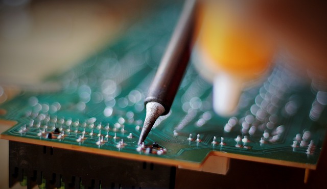
PCB components using surface mount technology derives major benefits from the associated automation and process controls available. For instance, it is possible to pack these PCB components close together on an electronic circuit board. Although most of the soldering work during assembly of printed circuit boards uses reflow techniques, certain components require soldering them manually.
While the high degree of automation involved with SMT does reduce the necessity of repair, and with careful attention to details, also reduces the requirements of touch-up and rework, it does not eliminate them. The electronics industry has already accepted rework and repair as part of assembling through-hole components on printed circuit boards. Although not a necessity, the SMT assembly manufacturing process also does require manual soldering in certain cases, such as for:
- Mounting temperature sensitive components
- Touch-ups
- Rework
- Repairs
Mounting Temperature Sensitive PCB Components
Using typical lead-free reflow profiles. a printed circuit assembly traveling through a reflow oven may take about 400 to 500 seconds from entry to exit. During this time, the board may experience a temperature rise of around 150 °C in the first 250 seconds, thereafter rising to a peak temperature of about 240 °C within the next 100 seconds. While most PCB components can easily survive this temperature-time excursion, some components, especially crystal controlled oscillators cannot, and tantalum chip capacitors may exhibit pop-corning effects.
PCB Trace. leaves out such temperature sensitive components from the electronic circuit board assembly, while the rest undergo reflow soldering. We mount the left-out components later, using temperature controlled manual soldering irons, taking care to complete the soldering work in the shortest possible time.
Touch-Ups
Ideally speaking, touch-ups should not be necessary in an automated assembly process during PCB production. A touch-up is necessary when the inspection of an electronic circuit board assembly reports some components to be without adequate solder to anchor them or with excess solder. The operator must touch-up or solder such components manually. There may be many reasons for components requiring a touch-up after a reflow:
- Stencil related
- Component related
- Design related
Stencil Related
SMT component manufacturers specify the proper opening for the stencil aperture for their components. If the aperture in the stencil does not conform to the specifications, the amount of solder paste deposited may be less than or more than what the component requires for proper soldering.
If the solder amount is too high, the component may float on the solder above the board, leading to height issues or issues like shorts with neighboring components. On the other hand, low amounts of solder may cause dry soldering on the component terminal, leading to an intermittent or open circuit conditions. Both conditions require a touch-up after inspection has confirmed the status.
Component Related
Sometimes the terminals of a PCB component may have tarnished, leading to low wetting during reflow soldering and resulting in intermittent or open circuit conditions. The operator may require application of additional flux to the joint while touching it up.
A similar situation may happen if the component size does not match with the pads on the printed circuit board. The component may be bigger than or smaller than its footprint pads on the board, leading to inadequate soldering.
Design Related
There are several design related issues requiring touch-ups afterwards. Most common among them are:
- Pads Mismatch
- Shadowing
- Solder Bridging
- Edge Placement
Pads Mismatch
A common design related problem that assemblers face during reflow is the tombstone effect. This causes a two-pin component to lift on one of its sides just like a tombstone does. The reason for this is the difference in size between the pads for the component on the PCB. Normally, designers place identical pads for a component on the board. However, if the pads are of different dimensions, the larger pad will have more solder on it and its surface tension will pull the component away from the smaller pad, lifting it in the process.
Shadowing
The design of a printed circuit board may place a large PCB component close to several smaller ones. This can lead to the large component overshadowing the smaller, preventing them from heating up adequately for melting the solder paste. This can lead to inadequate soldering on the smaller parts, requiring a touch up later.
Solder Bridging
PCB components placed too close together, and with inadequate solder mask dam between adjacent pins, can lead to solder bridging. This requires touching up to remove the bridging.
Edge Placement
Manual handling of circuit boards is common for inspection after component mounting and before the board enters the reflow oven. If the designer has placed components very near the edges, such components can move when handling the board, leading to touch-up requirements later.
According to our experience at PCB Trace., the above problems are more common during PCB prototyping services rather than in full-scale production. Usually, designers ensure resolving all such problems before the board enters the final production stage.
Rework
Under certain conditions, an operator may have to rework or replace a component or several components after completing the reflow process of a printed board assembly. These include placement of:
- Wrong Components
- Wrong Orientation
- Defective Components
Wrong Components
Placement of wrong PCB components may be an error in the BOM or programming error of the pick-and-place machine. Rectification of such errors may require de-soldering and removal of the wrong component and soldering in the correct one.
Wrong Orientation
Bipolar components like diodes and LEDs are usually susceptible to such errors in the silk-screen design or in programming the pick-and-place machine. The operator must de-solder and remove the component and solder it after cross-checking its correct orientation.
Defective Components
Some PCB components are more susceptible to damage from handling or heat. One of the common causes of active component failure during handling stems from inadequate implementation of ESD precautions during electronic circuit board assembly. Exposure to heat inside the reflow oven is another cause for failure of some sensitive components.
In both cases, the operator must replace the defective component identified during testing with a working component.
Repairs
Although repairs and rework may be similar in functionality, the former refers more to field failure returns. Defective PCB components in printed circuit board assemblies returned from the field (for whatever reasons) need replacement by manually de-soldering them and replacing them with their operating counterparts.
Read About: Should You Move to SMT PCB Assembly?
Conclusion
According to our experience at PCB Trace., printed circuit board assemblies that have not been touched-up, reworked, or repaired have a much higher success rate at testing and final use, in comparison to assemblies that have undergone manual soldering. It is common to experience failure of repaired PCB components and touched-up solder joints, including failure of parts and solder joints close to repairs. Use of modern SMT offers a suitable opportunity for reducing the necessity of touch-ups, repairs, and rework as a part of PCB manufacturing and assembly.
