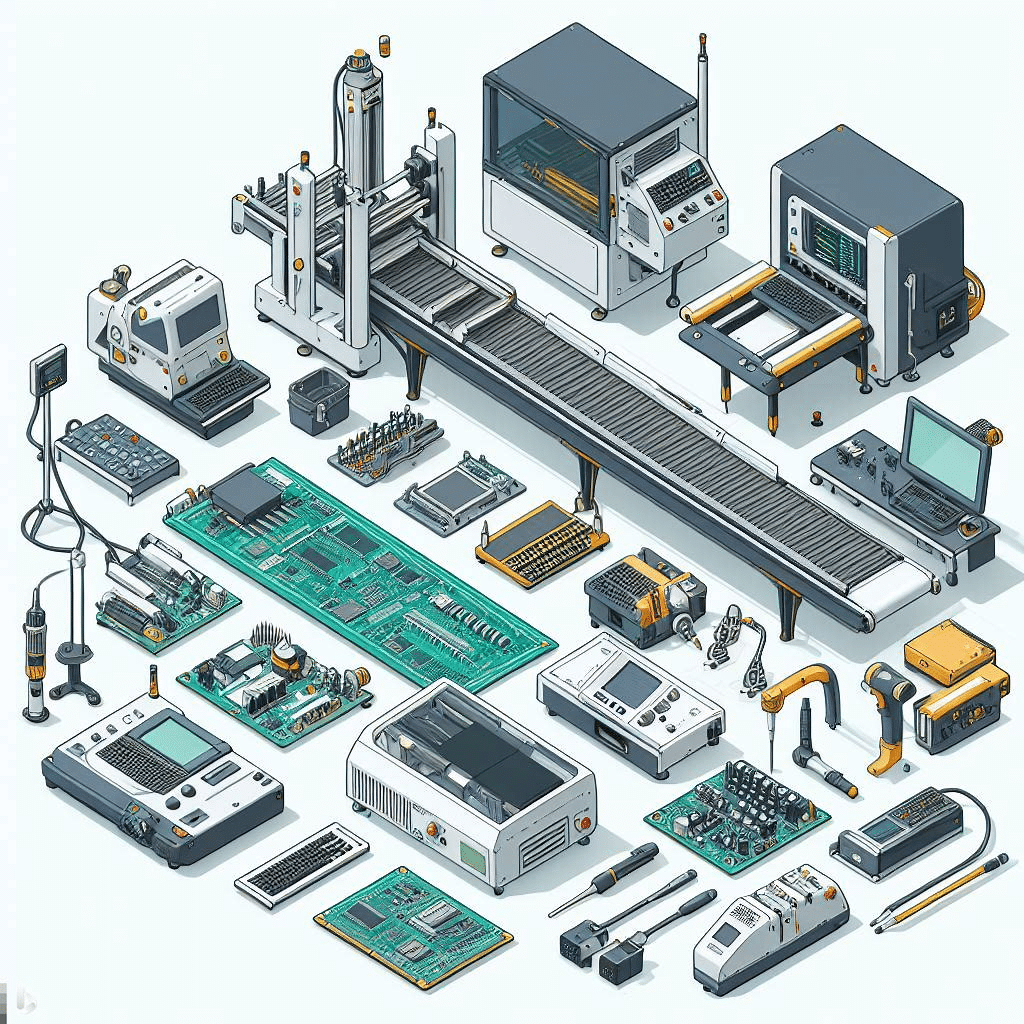
The PCB or printed circuit board manufacturing process is a complex procedure requiring many crucial steps, starting from design, proceeding through the production of the boards, and ending in their packaging and delivery. PCB Trace Technologies Inc. is a renowned PCB manufacturer, and we use computer-guided and automated machinery to ensure accuracy and efficiency in the PCB fabrication process. We also have many quality checks to guarantee high-quality standard PCBs.
Here, we reproduce the required steps for the PCB manufacturing process, detailing the procedures and machinery involved in each.
Design and Output
The initial step of the PCB manufacturing process starts with design. The first step in the design process is making the schematic layout that guides the fabrication of the board. The schematic is basically a plan containing all the requirements of the intended design. Designers typically use computers with PCB design software for drawing the schematic.
Commonly available PCB design software includes OrCAD, Altium Designer, KiCAD, Eagle, and PADS. Most design software produces design output in standard formats known as Gerber or Extended Gerber. Gerber/Extended Gerber formats encode the vital information in the design for presentation to the PCB manufacturer.
Once the PCB manufacturer receives the Gerber/Extended Gerber files, they perform checks like DFM or Design for Manufacturing. This ensures the design fulfills the basic requirements for manufacturing.
PCB Manufacturing
Printing the Design
After ascertaining the design checks, the manufacturer proceeds to print the design files. They use a special printer known as a plotter for this purpose. The output is a film showing all the details and layers of the board but in the form of a photo negative. The layers of the board show up as black opaque colors for copper conductive traces and pads, whereas the non-conductive parts remain clear.
After printing, the operator lines up the films and, using a punching machine, punches a registration hole through the films. This hole functions as a guide for aligning the films in later processes.
Printing Copper Circuits on Layer Pairs
The actual PCB production process begins from this step onwards. The manufacturer uses a copper-clad laminate that has a copper foil bonded to both sides of a dielectric substrate to form a layer pair. They coat the copper foils with a photo-sensitive film known as resist. The resist has photo-reactive chemicals that harden when UV light falls on them.
The manufacturer then places the respective layer films on the resist and aligns them to the copper-clad laminate. Exposing the combination to ultraviolet rays allows the rays to pass through the clear part of the film and fall on the resist, while the black, opaque parts of the film block any ultraviolet rays from passing through.
The UV light falling on the resist solidifies the photoresist in those areas, while the unexposed parts remain unaffected. The manufacturer then washes the board with an alkaline solution and again with pressurized water. This removes the excess unaffected and unwanted photoresist from the copper surface.
Etching the Layer Pair
In the next step, the manufacturer removes the unwanted exposed copper from the board surfaces. They do this by applying a chemical solution to the board that dissolves the exposed copper, leaving intact the copper portion covered by the solidified photoresist.
Resist Stripping
After the etching process completes, the manufacturer strips or removes all the hardened resist from the copper surfaces to form the circuit of the inner layer pair. They also perform a visual inspection of the board to inspect the circuit on the layers. For the inspection, they use a backlighted magnifying glass.
Post Etch Drilling
Using the registration hole as a guide, the manufacturer then aligns the layer pair to a computer-controlled optical punch machine. This machine punches the vias and other holes as necessary for this layer pair. Other machines, like laser drilling machines, may also be used for creating blind, buried, or microvias.
Automated Optical Inspection
The manufacturer then inspects all inner layer pairs made this way using an automated optical inspection method. A video camera attached to a computer searches for defects in the copper circuit pattern on the board layers. They repair any defects and compare the result with the Extended Gerber Design. If they match, the board proceeds to the next step.
Layer Pair Alignment
This step stacks multiple layer pairs for alignment. The manufacturer places a layer of pre-coated epoxy resin called prepreg between each layer pair. On both sides of this, they place another sheet of prepreg followed by another layer pair. They do this for all the layer pairs. Lastly, they place a press plate and send the combination to a lamination press.
Composite Circuit Board Lamination
The laminating press applies heat and pressure to the layers to melt the epoxy within the prepreg and allow all the layers and the prepreg to fuse together. After they are fused to form a composite circuit board, the manufacturer removes the press plates for drilling.
Adding the External Layers
In this step, the manufacturer adds the two outermost layers. These are two single-sided copper clads to form the top and bottom-most layers. They subject the entire board sandwich to heat and pressure, causing the epoxy to resist melting and bonding the layers together.
Printing Copper Circuit on External Layers
The manufacturer now prints the circuit on the two external layers by the same process as for the inner layer pairs and exposes them to UV light.
Drilling Through Holes
For drilling through holes, the manufacturer aligns the circuit board using its registration holes and uses an X-ray machine to pinpoint the spots for the drilling. A computer-guided drilling machine then follows the Extended Gerber design to drill the holes through the entire stack up. Apart from through holes, other vias, non-plated holes, and mounting holes for mechanical parts are also created in this step.
Plating & Tinning
After completion of the etching process, the manufacturer cleans the board thoroughly and uses a plating bath to plate the circuitry on the exterior layers of the board along with all the drilled through-holes with a layer of copper. After the plating, they cover the exposed copper with a layer of tin for protection.
Etching the Outer Layers
Finally, the manufacturer strips off the hardened photoresist from the board and etches away the unwanted copper chemically.
Removing the Tin
In this step, the manufacturer removes the protecting tin from the copper. This completes the primary fabrication of the circuit board.
Outer Layer AOI
Just like the inner layers, the manufacturer conducts an automated optical inspection for the two outermost layers. This confirms that the two layers are conforming to the design and do not have either extra copper or missing copper on the surface.
Solder Mask Application
After cleaning the board thoroughly, a machine applies an ink epoxy to each side and aligns a solder mask film on them. The board undergoes exposure to UV light that fixes the necessary pattern of the required solder mask on the board. The manufacturer then places the board into an oven to bake and cure the required solder mask on the board.
Silkscreen Application
Using an inkjet printer, the manufacturer prints the necessary legend on the PCB. This includes part numbers, warning labels, manufacturer’s logo, and ID numbers.
Surface Finish
The manufacturer finishes the PCB by covering the exposed copper on the board’s surface with conductive materials. This has a dual function, one of protecting the exposed copper pads before they are soldered and providing a reliable connection between the PCB and the electronic components.
PCB manufacturers must use Pb-free surface finishes in accordance with RoHS and WEEE.
Electrical Testing
For checking the PCB electrically, the manufacturer performs various tests following the standards of IPC-9252. They test the PCB for circuit continuity, shorts, and opens. They typically employ two machines for these tests—In-Circuit Tester and Flying Probe Tester.
The In-Circuit Tester has a fixture with numerous test probes. The operator places the board on the test probes and applies pressure on it to allow the probes to connect with the test points on the board. By applying known voltages to the probes and measuring the currents between them, it is possible to test for continuity, shorts, and opens in the board. The In-Circuit Tester is useful for high volume production of PCBs.
For small to medium-volume production, the Flying Probe Tester is more common for checking electrical performance. The machine has two or four test probes and uses a test program to connect them to specific test points for checking continuity, opens, and shorts on the PCB.
Profiling and Routing
In this step, the fabricator isolates individual PCBs from the panel. They cut them using a routing machine by scoring or making v-marks on the board according to data in the Gerber files. Some fabricators use CNC machines for this purpose. These machines create small cuts along the edges of the board, making it easier to detach them by breaking them without causing damage.
Packaging and Delivery
This is the last stage of PCB manufacturing. The operator covers the PCBs with a sealing material that keeps dust and moisture out. They pack the sealed boards into suitable containers to protect them during shipping and delivery. For large-scale production, the protection and packing are done using suitable machines.
Conclusion
At PCB Trace Technologies Inc., we use automated machines for PCB manufacturing mainly for their enhanced reproducibility, accuracy, and reliability. With so many intricate steps during the manufacturing of PCBs, human error can very easily ruin numerous boards very quickly. Machines help us avoid these errors, and we can confidently take up large-scale production, ensuring the highest quality and reliability of our printed circuit boards.
