Almost all electronic equipment contain a PCB or printed circuit board for providing a mounting space for various electronic components. Apart from a safe and sturdy mounting arrangement for the components, a PCB also provides pathways that electrically connect them, thereby allowing them to function together. With the advancement of electronics, form factors of electronic equipment are shrinking, resulting in reduction of space on PCBs. Accordingly, PCBs, like those made by PCB Trace Technologies Inc, are changing over to a sandwich of multiple layers for providing the necessary connections.
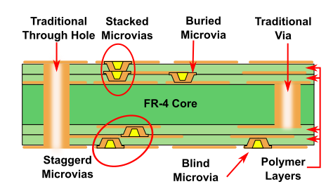
Multiple layers require routing electrical connections between them. Manufacturers use vias or drilled holes that often pass through the board. When they plate the holes with copper, they make connections to the necessary layers to interconnect them. These are PTH or plated through holes or plated through vias. Other forms of vias are also in common use—blind and buried—which do not pass through the board. While buried vias connect two or more internal layers, blind vias connect one of the outer layers with one or more internal layers. Sophisticated HDI or High Density Interconnect boards use very small diameter vias that need drilling with lasers rather than mechanical drills. These are micro-vias.
Benefits of Micro-Vias
The IPC or Institute of Printed Circuit Boards defines a micro-via as a hole in a PCB with an aspect ratio of 1:1, and whose depth does not exceed 0.01 inches or 10 mils. Using modern lasers, it is possible to drill such tiny holes easily. However, as micro-vias have limited depth, they can interconnect only two adjacent layers within a multi-layered board. This leads to several special arrangements for building up blind and buried via connections using micro-vias:
Stacked Micro-Vias: Manufacturers can stack several micro-vias on top of each other, thereby allowing interconnections between several adjacent layers.
Staggered Micro-Vias: Manufacturers can also interconnect layers by using multiple vias staggered or placed as offset from one another rather than stacking them on each other. This has the advantage of providing more space for routing, as compared to stacked micro-vias.
In-Pad Micro-Vias: This involves placing a filled micro-via directly on the copper pad, allowing substantial miniaturization of the PCB.

PCB designers benefit substantially when using micro-vias in their circuit board designs, as micro-vias provide thermal and mechanical reliability to the performance and functioning of the board. Furthermore, in-pad micro-vias allow increased miniaturization, especially with circuit boards becoming lighter and smaller, such as for fitting into mobile devices. With sizes much smaller than regular vias or plated through holes, micro-vias save space extensively on the circuit board. The designer can target a much smaller board to fit all the components.
Using micro-vias reduces the risk of defects also. Regular vias need mechanical drilling, which cannot go below a certain diameter. On the other hand, micro-vias are much smaller, as they are made using lasers. As the PCB size reduces when designers use micro-vias, the trace length are also shorter, leading to less fabrication issues. Signal integrity improves significantly with shorter traces and smaller vias—a huge benefit when making HDI or High Density Interconnect boards. High speed circuits benefit largely from the use of smaller vias, as large vias produce higher amounts of radiation. In-pad micro-vias enhance the EMC characteristics of the board, while improving the RF capabilities and reliability.
Considerations when Designing with Micro-Vias
When creating micro-vias on PCBs, designers must take care of several aspects. The most important of them is it should be possible to plate the hole. For a reliable plating, the aspect ratio or hole diameter to depth ratio must not go above 1:1. Drilling with a mechanical drill may result in a larger aspect ratio, but the hole will not be reliable as the plating will be defective.
Typically, PCB designers prefer to not go below a diameter of 4 mils irrespective of the aspect ratio, when drilling a copper surface of the PCB with a laser drill. For laser drilling, a copper weight of ½ oz is an ideal choice, as it is difficult for laser beams to drill into thicker copper and ablate down to the next layer.
Micro-vias in internal layers of multi-layered boards require an additional lamination step. Manufacturers usually fill unused holes with non-conductive epoxy, or they may plate them over totally. Copper is a common material for plating, and as micro-vias are so small, most manufacturers do not fill them. Plating the vias requires a specialized bath and chemistry, and this provides more flexibility.
If a micro-via connects two layers, while skipping a layer in between, the middle layer must have a clearance as the via passes through. Designer can use staggered or stacked vias when connecting three layers in continuity. For manufacturers, it is easier to create staggered micro-vias, and they provide the board with greater reliability.
Designers must also consult PCB manufacturers for the materials they must use when designing with micro-vias. This is because some materials are more suitable for creating micro-vias using lasers. Not only do micro-vias offer substantial flexibility to designers, they also enhance the reliability for multi-layered printed circuit boards.
Conclusion
PCB Trace Technologies Inc recommends discussing with the PCB fabricator at the earliest stages of the design process. This allows the designer to understand the options available to them and choosing the most optimum among them. We have experienced engineers for helping our customers select the best material for their HDI and micro-via design. Our customers benefit from the smaller boards as a result of using micro-vias. The overall cost of the smaller boards often turns out to be lower, along with lower risks and higher reliability.
