Introduction
PCBs or Printed Circuit Boards are the fundamentals of electronic equipment. Product development often requires engineers to typically test and validate their concepts by building prototypes. Successful evaluation leads to the launching production of PCBs at volume. According to eminent PCB manufacturer PCB Trace Technologies Inc., many critical differences exist between prototype PCBs and volume PCB production. It is essential to understand these key contrasts for businesses to transition smoothly from design validation to mass production.
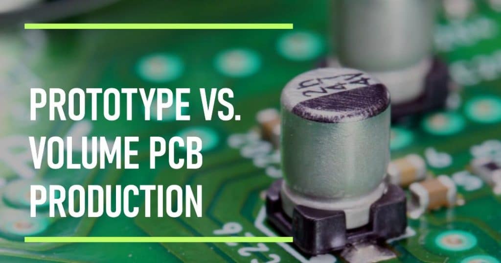
What are Prototype PCBs?
Prototype PCBs are boards that engineers require for testing the functionality and verification of their concepts. The focus is majorly on fast turnaround times over shorter fabrication runs. Creating a PCB prototype allows them to physically validate and test their circuit design, as against relying on simulations that may never be able to fully predict all the potential issues that could arise in the real world. Additionally, with a physical prototype, engineers can identify and address design flaws that they would otherwise have overlooked.
Difference between Prototype and Volume PCB Production:
The major differences between prototype and Volume PCB Production are as follows:
Quantity
The quantity of boards during prototyping is substantially smaller than that involved in mass production. For instance, the ratio could be 5:10,000 on the low side.
Cost per board
The cost per board for prototypes is typically higher than the cost per board in production. This is primarily due to the inefficiencies involved in producing a smaller number of boards.
Lead Time
Lead times for both fabrication and assembly of prototype boards are much smaller mainly due to their smaller numbers, than that involved in producing a larger number of boards.
Design
The design of prototype boards is typically less complex than that of boards suitable for mass production. This is due to prototypes being used primarily to test and validate concepts, whereas mass production requires boards suitable for high throughput.
Testing
Testing of prototype boards is mainly to establish functionality and validate concepts. On the other hand, testing of mass production boards is primarily to establish reliability.
Quality
The quality of prototype boards is not a concern as their requirement is only for a short duration. Hence, prototype boards are often lower in quality in comparison with production boards which must necessarily be of a higher quality to survive for much longer durations.
Materials
Prototype boards may use materials that are generally less expensive in comparison to those that mass-production PCBs require. This is due to the requirement of prototype PCBs to only establish functionality and validate concepts. On the other hand, production PCBs require more expensive materials as they must maintain their quality and satisfy requirements for a longer period.
Key Factors Influencing PCB Pricing
Whether prototypes or mass production PCBs, understanding their cost is like
piecing together a complex puzzle. Various elements and factors intertwine to
generate the final cost, with each contributing its unique influence. These
factors are — Material selection, Design complexity, Volume, Quality, and
Testing requirements.
Impact of PCB Materials
Material selection contributes the most towards the overall costs of PCB manufacturing. The breakdown is as follows:
1. Base Material
This is the substrate material, primarily dependent on the application type. For instance, general-purpose PCBs may be made of standard FR4, costing around $2-$3 per square foot. On the other hand, high-frequency PCBs may require using Rogers 4003C, costing approximately $25-$30 per square foot.
2. Copper Thickness/Weight
This is the thickness of the copper foil on the PCB substrate and may range from 0.5 oz to 3 oz or more per square foot, dependent on the current flow requirements. For instance, 1 oz of copper weight costs about $3-$5 per square foot. Doubling the copper weight can increase the costs by about 20- 30%.
3. Surface Finish
Again depending on the application, you can use options like HASL or hot air solder leveling costing around $0.05-$0.10 per square foot. On the other hand, the use of superior performance surface finishes like ENIG or electroless nickel immersion gold can increase the cost by as much as $0.2 per square inch.
Production Process Efficiency
Production processes that manufacturers employ can alter the cost structure of the PCB as follows:
1. Manual Vs. Automated Processes
While manual soldering can cost up to $0.05 per joint, it is a slow process and depends on the complexity of the board. On the other hand, automated assembly lines can be significantly faster, while costing around $0.01 per joint.
2. Turnaround Time
A standard production time involving a 10-day turnaround may add no additional cost. On the other hand, expediting the production to a 48- hour turnaround can increase the costs by 40-50%.
3. Testing and Quality Assurance
Depending on the complexity and required precision, rigorous testing procedures like AOI or automated optical inspection can easily increase production costs by about $0.10-$0.20 per square inch.
Design Complexity
PCB Design complexity is yet another significant cost driver. Major influencers are:
Layer Count
While a single-layer PCB may cost around $0.10 per square inch, a four- layer board may cost upwards of $0.30 per square inch, depending on the complexity of the design and the quantity ordered.
Via Types
PCBs with through-hole vias are less expensive and may cost around %0.01 per via. On the other hand, the use of blind and buried vias can increase the cost to about $0.02-$0.05 per via depending on the additional processing steps necessary.
Trace Widths and Spacing
Tighter tolerances for narrower trace widths and spacing may raise the cost by about 10-20% due to more precise manufacturing processes necessary.
Impedance Control
High-speed applications require impedance control for maintaining signal integrity and minimizing EMI. This requires following strict design rules, and using specialized materials, and this can increase the PCB cost by about 20-30%.
Impact of Volume
Scaling up the production volume substantially reduces the cost per unit board. For instance, scaling up by a factor of 10 from an initial volume of 100 may lower the cost per unit by about 30-40%.
Cost Comparison Between Prototypes and Volume PCB Production
| METRIC | PROTOTYPE | LOW VOLUME | HIGH VOLUME |
| Quantity | 1-5 PCBs | 10-100 PCBs | 1000+ PCBs |
| Lead Time | 5-10 Days | 10-20 Days | 4+ Weeks |
| Tooling Costs | Minimal | Moderate | High |
| Materials | FR4 | Rogers 4003C | Rogers 4003C |
| Production Process | Manual | Automated | Automated |
| Testing | Visual | AOI | AOI |
| Design Complexity | Same | Same | Same |
| Surface Finish | HASL | ENIG | ENIG |
| Cost per board | Very high | Moderate | Low |
Techniques for Optimizing PCB Cost
Some techniques that designers use to optimize or reduce PCB costs:
- Using the lowest acceptable substrates that meet requirements
- Eliminating unnecessary layers
- Consolidating components to minimize board size
- Increasing routing densities while maintaining clearances
- Relaxing tolerances wherever possible
- Standardizing common materials, board sizes, components, and finishes
- Reusing proven implementation approaches
- Working with fabricators to improve manufacturability.
Implementing the above, along with a collaborative design approach with fabricators and assemblers can balance performance needs while rationalizing cost realities along the development process.
Conclusion
According to PCB Trace Technologies Inc., estimating PCB manufacturing costs accurately requires a thorough understanding of the multiple factors contributing to the fabrication process. Although performance is crucial, designers must also evaluate the implications on cost due to material selection, stackup, tolerances, and volume.
This allows them to strike the optimum balance between capabilities and price. Guidelines offered in this article provide confidence to engineers in making effective design trade-offs and predicting PCB costs to meet project needs.
Frequently Asked Questions
What is Rapid PCB Prototype Services?
Some manufacturers offer rapid prototype services to offer small batches of prototype boards with exceedingly fast turnaround times, sometimes as fast as 24-48 hours. The service often accommodates late engineering changes with fast respins.
How long does it take to make prototypes?
Typically, fabricators produce a small batch of prototype boards very quickly, sometimes as fast as 24-48 hours.
Is prototyping really necessary?
Prototyping is a crucial step during PCB design and development for engineers to verify and validate their design. They use prototypes when building new PCB design projects, and also during design updates or revisions.
Are there any requirements for making PCB prototypes?
The requirements are the same as for any PCB project. You must provide PCB design files, Bill of Materials, stackup details, DRC, Test requirements, and other instructions.
What do you mean by high volume PCB production?
High volume PCB production typically involves quantities of at least hundreds if not thousands of boards.
