The next generation wireless networking technology, namely 5G or fifth generation, is expectedly going to change the way people live and work. Compared to the latest technology today, the 4G LTE, 5G will be faster and capable of handling significantly more connected devices. Although 5G networks have started rolling out around 2018 in the US and other parts of the world, the technology is still is in its infancy. However, the industry has a huge potential.
PCB Trace Technologies Inc. understands the impact that 5G will have on electronic devices. There will be profound impact primarily on data traffic and faster data rates—implying requirements of significant manufacturing innovations for handling the demand for scale and quality. Almost all industries will feed the impact of 5G, starting from entertainment to mobile phones to industrial applications and transportation. However, the biggest impact is likely to be on the PCB manufacturing industry, as printed circuit boards are the basis of all electronic products.
The reason for this impact is the operating frequency—5G devices operate in frequency bands at least five times higher than 4G devices do. The higher frequency bands allow 5G networks to transfer more data at faster rates, around 100 times faster than 4G networks can. At such high frequencies, everything is smaller, including components, board size, and interconnections, while performance of the signal as it travels across the board becomes paramount.
If not handled correctly, the degradation of signal in the PCB can delay the transmission, and impact data flow at the same time. PCB designers and manufacturers must ensure proper signal integrity in their design and fabrication of circuit boards. PCB Trace Technologies Inc. is handling such issues with the use of mSAP or modified semi-additive processes. The mSAP process ensures creation of traces with precision cross-section, leading to better impedance control and signal integrity.
Subtractive and Additive Manufacturing Processes
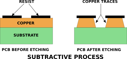
PCB manufacturing conventionally uses subtractive processes during fabrication. In the etching process, chemicals remove unwanted metal from copper clad substrates, leaving behind traces to carry the signals. Controlling the etching process is difficult, and results in variations in the cross-section of the traces along their length. The inconsistency in the cross-section affects the impedance of the traces, more so for 5G signals, as they are higher in frequency, resulting in higher signal loss.
The additive mSAP process ensures formation of traces with perfectly vertical walls and consistently rectangular cross-section throughout its length. While the process lowers signal loss for 5G, mSAP also helps to improve circuit density. IC manufacturers typically use the mSAP process for making substrates, and PCB Trace Technologies Inc. has adopted the modified semi-additive process for the HDI PCB industry.
At present, with subtractive processes, achieving track width/space dimensions of 3/3 mils is easy, and we can go down to 2.5/2.5 mil. With mSAP we can go down further to 2/2 mil, thereby allowing 5G smartphone manufacturers to achieve tremendous device densities, while taking advantage of superior geometries of traces and accurate impedance control at high-frequency operation.
Etching Versus mSAP
The etching or subtractive process uses an etch-resist coating on the copper layer, applying a photolithography process to map form an image of the areas of copper necessary to retain, while chemically etching away the unwanted and unimaged copper.

Although the chemical treatment creates vertical tracks on the substrate, the process also dissolves copper in the horizontal direction along the track walls. The cross-section of the resulting track therefore, appears trapezoidal and uneven along the length. The wedge-shaped track introduces several impedance anomalies, while compromising circuit density as the lines in some places are wider than intended.
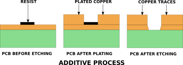
In contrast, mSAP is an opposite technique, an additive process. Here, we plate a thin copper layer on the laminate, and after the photolithography process as before, add more copper by plating in the areas where the resist is not present. This is the additive part in the process. After achieving the necessary copper thickness, we remove the resist and chemically etch away the remaining thin layer of copper between the traces.

While the subtractive process defines the trace geometries during etching, the mSAP process defines them during the photolithography process. This allows formation of traces with much greater precision, with the sides in straight vertical lines. The consistency in the rectangular cross-section allows forming traces closer, thereby achieving maximum circuit density, while enabling accurate impedance control, better signal integrity, and lower signal loss.
Beyond mSAP
Although mSAP helps us PCB manufacturers overcome the technical hurdles when producing HDI boards for 5G, we implement it in a manner that maximizes production throughput while minimizing the costs. This way, we ensure there is adequate return on our investments.
Typically, IC substrate production uses the mSAP process, as their huge production numbers allow absorption of the higher costs associated with mSAP. In PCB manufacturing, the commercial volume scales being much lower, the costs of implementing mSAP are higher, warranting higher production efficiencies.
Therefore, while transitioning from 4G to 5G, although we are effectively employing mSAP in mass production, PCB Trace Technologies Inc. is also investing in advanced manufacturing tools and techniques for maintaining and extending our competitive advantage.
With mSAP, we are targeting HDIs with precisely formed traces and very high densities. For this, we are adopting advanced forms of direct imaging or DI systems. Direct imaging allows us to achieve traces with width down to 0.4 mils and spacing of 0.6 mils. To ensure precise uniformity, we need to maintain a very high registration accuracy of 0.3 mils.
Read About
What is a Hybrid PCB?
Reducing Automotive PCB Defect Rates
Conclusion
PCB Trace Technologies Inc. is tracking the evolution of 5G and adopting new techniques for advanced HDI PCB manufacturing using mSAP, DI, AOI, and AOS technologies for lowering manufacturing costs, accelerating throughput, and maximizing PCB yields.