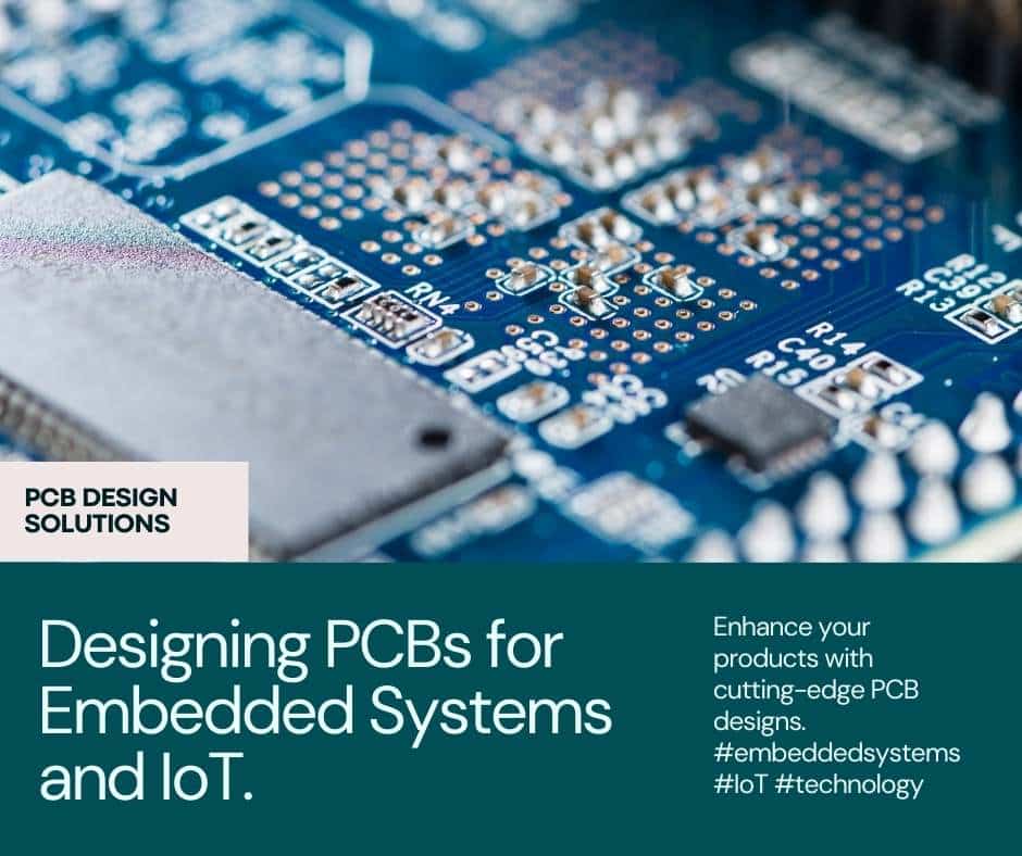
We live in an interconnected world. Here, embedded systems and IoT, or the Internet of Things, are an integral part of our lives. Not only homes and wearables, IoT and embedded devices are revolutionizing many industries as well. As most of these devices are small, designing them effectively requires careful attention and consideration of details. Most PCBs for embedded systems and Internet of Things devices possess several characteristics distinguishing them from traditional PCBs. Designers tailor such characteristics to meet specific requirements of low-power, compact, and interconnected devices.
Here, we, at PCB Trace Technologies Inc. explore essential design hints to help unlock the full potential of such connected devices.
What are Embedded Systems?
Embedded systems are electronic products based on microcontrollers. They typically possess memories, computational logic, communications, and I/O peripherals. Embedded systems are typically for a specific function. For, instance, a washing machine is an embedded system, and so is the security access system, a smartphone, a vending machine, and many other intelligent appliances.
What are IoT Devices?
IoT devices are individual non-standard devices with computational abilities. They typically integrate sensors, actuators, and appliances and connect to a network wirelessly to transmit data. Having both industrial and consumer uses, IoT devices typically integrate into other devices like medical devices, industrial equipment, and mobile devices. They can be a part of embedded systems also. IoT devices can often send data or interact with other devices over a network.
What is the Design Cycle of Embedded Systems and IoT devices?
While both are small devices, tackling their design requires a good plan and a systematic approach to breaking down the design cycle into manageable stages. This allows proper execution and collaboration. The design plan must include:
Requirements Collection
While designing embedded systems and or IoT devices, the first crucial stage is to gather and analyze product requirements before turning them into specifications. It is necessary to list out all individual requirements and clarify them with your customer.
Apart from the logic diagram and the number of I/Os in the embedded system design, it is also necessary to probe into the operating conditions and usage to determine the right specifications. For instance, an embedded system or an IoT device that works in an indoor environment can be very different from those that need to reliably work in harsh external conditions.
Schematic Design
After translating the requirements into specifications, the designer can start building the schematic. At this stage, the designer must choose the right microcontroller and other components for the PCBs for embedded systems and Internet of things.
Component Selection
The designer must select components that are energy-efficient and compact. They must also be compatible with the selected communication protocols.
As PCBs for embedded systems and IoT devices must withstand a range of environmental conditions, the designer must select components that are resilient to these environmental conditions. Therefore, the choice must include considerations for temperature changes, humidity, and other factors that the device could encounter when operating in various operating environments.
As the microcontroller is the central component in an embedded system, the designer must select it with due consideration. They must consider factors like processing speed, memories required, peripherals necessary, power consumption, and finally, the cost.
PCB Materials Selection
This is also the correct stage for selecting the material of PCBs for embedded systems and Internet of Things devices to allow it to withstand a wide range of environmental conditions. For instance, it may be necessary to choose a material with good thermal conductivity, as this helps in thermal management.
PCB Design
After completing the schematic, selecting the components, and the PCB materials, the next task for the designer is to design the PCB. Being a delicate process, the designer must apply the best practices for obtaining proper functionality, manufacturability, and reliability from the PCB.
The design of PCBs for embedded systems and Internet of Things devices may get complicated when using a high-speed controller and/or mixed-signal circuits. High-speed designs often involve problems like EMI, and designers must provide noise-coupling mitigation measures and proper ground separation for mixed-signal designs.
Compactness
Most IoT and embedded systems tend to be small and more compact. PCB designers focus on reducing the overall form and size of the PCB without compromising its functionality. They use HDI or High-Density Interconnect to increase the component density with fine trace routing and smaller via sizes, thereby creating PCBs that are not only smaller but also feature-rich. HDI allows compact form factor designs and utilizes board space more effectively.
Most often, designers use multiple layers in their PCB design. With multiple layers, they can complete the routing more effectively while keeping a smaller form factor. Another advantage of multiple layers is they can use ground and power planes to effectively design a low-noise and more stable design. While multiple layers contain electromagnetic fields better, they also reduce the risk of EMI, thereby improving the device’s performance and its compliance with regulatory standards.
Most IoT and embedded systems, being compact, require PCB components that are small and able to fit in the space available. For this, designers commonly use SMT or Surface Mount Technology components because of their small form factor. Not only electronic components, designers must select smaller size connectors also to minimize the overall design.
In addition to using HDI technology to increase the component density, designers also go for flexible PCBs that can fit into irregularly shaped spaces. By bending and twisting, flexible PCBs accommodate the available form factor.
Low-Power Design
One of the primary requirements of embedded systems and IoT devices is they must manage power effectively. As many of these devices are battery-powered, they must consume power optimally to prolong the battery life. Designers must carefully design the PCB layout to minimize power consumption both during active and standby modes. They can do this by optimizing trace routing, strategically placing power planes, and using low-power-consuming components.
The design of most IoT devices allows them to spend a significant amount of their working time in sleep modes, consuming low power. The design of PCBs must support these modes by power gating techniques, which completely disconnect power from inactive components. This is easily achieved in PCB design by optimizing power distribution, using low power-consuming components, and resorting to sleep modes to maximize energy efficiency.
Wireless Connectivity
Most IoT devices and some embedded systems essentially use wireless connectivity to communicate. Designers must pay special attention to the antenna design to optimize its performance. Designers have the freedom to choose from a variety of wireless communication standards, such as Wi-Fi, LoRA, Zigbee, Bluetooth, and others. Their choice depends on the power, data rate, and range required by the application.
Thermal Management
Being of a small form factor, thermal management is an important feature of IoT devices and embedded systems. Most systems can generate a substantial amount of heat when operating, which may prove detrimental unless removed. Preventing overheating improves energy efficiency, maintains stable performance, and ensures overall longevity of all components. Thermal stress can enhance mechanical failures, and increase safety concerns. Moreover, thermal management is necessary for compliance with industry standards and regulations, and this is essential for market acceptance and product certification. In all, thermal management is necessary for optimizing device performance, safety, and lifespan.
Multiple Sensors
IoT devices and embedded systems often use various sensors to collect data. PCBs typically integrate dedicated sensors with interfaces. For accurate sensor data acquisition, designers may integrate signal conditioning circuits along with the sensor.
Many IoT devices require a mix of digital and analog signals. Designers must include the interface between these signals to minimize noise and interference.
Energy Harvesting
IoT devices must often reside in remote locations, where it is difficult to replace batteries. Designers use energy harvesting techniques to power these IoT devices, making them maintenance-free. They design the interface to capture and store harvested energy effectively. The PCB design must support and optimize these techniques, thereby enabling the device to operate with minimum external power sources.
Prototype Design
Once the PCB layout has passed the DRC tests and is free from errors, the designer gets prototypes made to test their design.
Firmware Development
PCB and hardware design is only a part of the IoT and embedded system design. Designers must use coding to make the hardware function as intended. They speed up the process by using existing driver libraries. They also use sample codes from manufacturers.
Debugging the code is a part of the process, making developing firmware a time-consuming process.
Testing and Acceptance
An IoT or embedded system must pass stringent tests before it can be approved for manufacturing and deployment. This includes passing not only functionality tests but also tests for reliability and safety.
What are the Challenges in IoT and Embedded System Design?
Every step in designing an IoT device or embedded system is important. However, the PCB design stage is the most crucial for a successful outcome.
- PCB Design: It is easy to fix bugs and other issues related to code by revising the firmware. However, once a PCB is manufactured and assembled, revising it for mistakes involves substantial amounts of time and cost involvement. Therefore, when designing PCBs for IoT or embedded systems needs careful design and test processes.
- EMI: Designers must prevent or minimize issues like EMI by implementing strict design rules. Running a thermal analysis on a PCB layout can uncover thermal heat points.
- Fitting: Fitting perfectly within the enclosure is another area where the designer must pay close attention. Designers can accomplish this by using proper PCB design and analysis software systems.
- Cost: As in all types of design, cost-effectiveness is one of the crucial considerations in designing PCBs for IoT and embedded systems. Designers typically focus on using cost-efficient components and manufacturing processes that do not compromise on performance, reliability, and quality.
- Modularity: Designers use modular designs with standardized connectors to easily integrate future sensors and modules. This allows them to achieve adaptability and scalability for different use cases. They also use standard communication interfaces like SPI or I2C for integrating third-party modules without significant reworking.
- EMC: To ensure devices can continue to operate without interfering with one another or being affected by external devices, it is vital to enforce EMC or Electromagnetic Compatibility in the design. For this, designers use grounding techniques, filtering, and shielding to reduce interference and ensure reliable operation.
- DFM: To minimize production costs, designers must design their PCBs with DFM principles in focus. For this, designers must consider ease of assembly, ease of testing, and ease of mass production to meet large-scale deployment requirements.
Conclusion
At PCB Trace Technologies Inc., we follow a holistic approach to designing PCBs for embedded systems and the Internet of Things. We consider factors like thermal management, signal integrity, wireless connectivity, and power efficiency. We also adhere to best practices, thereby developing reliable and efficient PCBs, meeting specific requirements of IoT applications and embedded systems.
