The development and manufacture of vehicles has always needed some printed circuit boards or PCBs. According to PCB Trace, with the advent of electric vehicles, the role that PCBs play has increased tremendously, especially for the advancement of the technology in electric cars.
A core part of the automotive industry requires the use of PCBs, essentially as computers are now playing an important role in making driving a more comfortable, convenient, and functional experience. Barring the vintage models, almost all cars now require a series of sophisticated electronic systems to operate their general functionality, safety, transmission, heating and engine controls, entertainment, GPS navigation, dashboard alerts, and much more.
Why PCBs Matter in Electric Vehicles?
Compared to traditional cars, an electric vehicle relies on many complex PCBs to power up, operate, and function. Recent years have seen enormous developments in the electronic industry. With increasing demands for additional energy savings and improved performance, the need for more sophisticated PCB solutions is also increasing.

Apart from the typical vehicle management, PCBs also play an essential role in voltage conversion, battery performance, and power conditioning in electric vehicles.
For instance, the latest electric vehicles use a new technology for converting waste energy during coasting and braking into driving power. PCBs harness this technology, and soon this feature will be commonplace enough for improving renewable credentials.
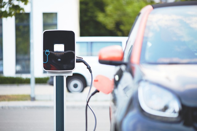
Charging stations play a significant role in furthering the use of electric vehicles by allowing reliable charging of electric vehicle batteries. PCBs are an important factor in these pay to charge units, helping the public charge their vehicles using an automated service for an inbuilt payment facility.
EV PCB Manufacturing Challenges
The environmental conditions within an operating electric vehicle pose the biggest challenge that PCBs must face when powering them. Other products and equipment can use fans, heat sinks, and heat spreaders to manage the heat output from the working machinery. However, electric vehicles do not have that luxury. Rather, designers and manufacturers must use special substrates that can perform at a higher level of thermal conditions.
For instance, regular resin boards cannot deal with the heat generated in electric vehicles. Manufacturers must use ceramic and reinforced glass PTFE to achieve the necessary stability under these thermal conditions. Innovative hybrid substrates are in development for offering a greater choice to the industry.
Types of PCBs in Electric Vehicles
The last few years have seen the development of various types of PCBs and substrates with a performance and cost advantage over ceramics. These PCBs can manage the power stage and control with a single substrate, whereas ceramic power stages require a separation of the control board and related interconnection architectures. Some innovative PCB technologies in the field of power electronic substrates are:
PCBs with Heavy Copper
The automotive industry has been using heavy copper PCBs for long, especially for relay- and fuse-boxes. With the increase in electrical power in vehicles, this technology is in revival. Using heavy copper PCB technology also helps to reduce the parasitic inductance of conductors by stacking one heavy copper layer over another in multilayer boards. With 12 oz or 400 µm of copper in the inner layers, it is possible to achieve a potential current carrying capacity of more than 1000 Amps. The outer layers of such heavy copper multilayer boards must not go beyond 150 µm, else the solder mask process will require additional efforts to achieve safer electrical insulation.
Heavy copper PCB technology has the disadvantage of being incompatible with fine-pitch copper structures, as it is difficult to etch fine pitch along with heavy copper. Therefore, power electronic systems typically use a heavy copper design for the power stage and a standard copper thickness for a separate control board using Surface Mount Technology. This requires a large installation space for hosting both boards, including connectors between them.
Combination Power PCBs
Combination power PCB technology offers a unique solution for the above situation. It combines heavy copper design and standard copper design in the same board. The technology makes it possible to install heavy copper in the inner layers alongside standard copper structures. A common outer layer in regular copper thickness provides the electrical connections for the entire board.
The insulating layers between the heavy copper layers often pose a barrier to optimal heat dissipation in the z-axis. Therefore, manufacturers prefer to use heavy copper technology only for managing high currents. For heat dissipation, manufacturers use alternate technologies like an insulated metal substrate (IMS).
Insulated Metal Substrates
IMS typically comprises a metal heat sink, a thin insulating layer, and a single copper layer on the top. This construction is suitable for simple designs that must host many heat generating components. More complex component arrangements require additional copper layers along with optimized heat dissipation.
Typically, lightweight aluminum as the metal offers a convenient solution, as it has high CTE. However, the introduction of copper as the heat sink metal improved the PCB reliability. Along with other characteristics, copper as heat sink also improves the thermal capacity.
Inlay PCB Technology
Shortening the distance between the power component and its heat sink leads to reducing the thermal resistance. Heat typically travels from a hot component mounted on the top surface of a PCB through the board to the heat sink along the z-axis. Manufacturers often laminate a massive inlay of copper element within the PCB to reduce the thermal resistance substantially. Even when not used for heat dissipation, such inlays are helpful for achieving a low ohmic resistance for high current flow.
Conclusion
According to PCB Trace, many innovations are under development for improving heat dissipation from the inner layers of the PCB to the heat sink. For instance, some manufacturers use power semiconductors assembled in lead frames to act as a heat spreader, thereby reducing the thermal resistance considerably. Most technology innovations strive to improve not only the heat dissipation, but also other electrical parameters.
