HDI or High-Density Interconnect technology has brought about a revolution in the PCB or Printed Circuit Board industry. It allows designers to create highly complex boards in smaller sizes but with improved performance. With the form factor of electronic devices reducing continuously, and greater functionality expected out of them, the significance of HDI PCBs is highly evident. According to eminent HDI PCB manufacturer PCB Trace Technologies Inc., optimizing board performance depends significantly on choosing the right HDI stackups, thereby determining its performance, cost, and reliability.
Depending on their capabilities and distinct advantages, designers have several HDI stackups from which they can select the most optimum one. However, when selecting the most ideal stackup for their application, designers must consider several factors like signal integrity requirements, component density, and objectives for thermal management. Moreover, they must also take into account budget and manufacturing constraints, as certain stackup types can be more challenging to produce than others, and hence, more expensive.
Here, we will be exploring the different HDI stackup types, the features that distinguish them, and how designers can determine the optimum choice for their PCB design needs. With a thorough understanding of the chosen HDI stackups, its benefits, and its limitations, designers can optimize their PCBs to deliver superior performance in the present technologically advanced world.
High-Density Interconnect PCBs
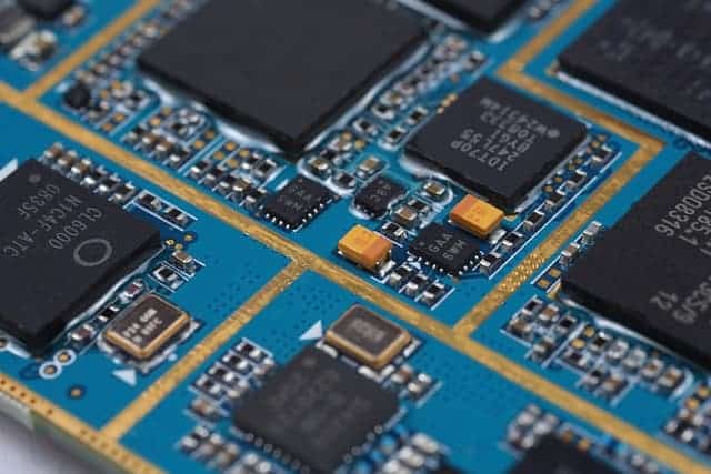
HDI or high-density interconnect PCBs are a special type of printed circuit board with their design allowing for very high component densities, resulting in more complex and compact electronic devices. One of the distinguishing features of HDI PCBs is the presence of microvias. Much smaller than traditional vias, microvias enable high-density routing, resulting in a higher component count in smaller areas.
Advantages of HDI PCBs
HDI PCBs offer several advantages including:
Higher Component Density
Capable of accommodating a higher number of connections and components in a given area, HDI PCBs lead to better space utilization and more compact devices.
Improved Signal Integrity
Shorter interconnections and small microvias in HDI PCBs improve signal integrity, resulting in faster signal transmissions.
Reduced Weight and Size
With HDI PCBs capable of fitting more components in smaller areas, the overall result is a reduction in device weight and size. This is important and essential for portable and handheld devices.
Enhanced Flexibility
HDI technology allows greater flexibility in PCB design during component placement and routing. That makes it easier for designers to handle complex circuitry.
HDI Challenges and Limitations
Although offering significant advantages, HDI PCBs are not without their typical challenges and limitations in their design and manufacturing stages. These include:
Higher Design Complexity
Higher component density and smaller form factors involve more intricate layouts when designing HDI PCBs. Designers can find this more challenging and time-consuming.
Higher Manufacturing Costs
Manufacturing complex PCB designs requires specialized equipment and materials. This leads to HDI PCBs having higher manufacturing costs as compared to conventional PCBs.
Limited Availability
Not all manufacturers may have the advanced materials and machinery required by HDI PCB manufacturing processes. Sometimes these materials can be difficult to source and may increase lead times.
HDI Stackup Types
Broadly, there are four popular types of HDI stackups. These are:
Passive Substrate
The Passive Substrate type of HDI stackup typically has a single HDI layer above or below the core layers. With this approach, the designer can have a lower PCB thickness compared to the thickness of a traditional multilayer PCB with the same number of layers. The higher density of interconnects is restricted to a single layer.
Benefits of Passive Substrate HDI stackup include:
- A single layer of high-density interconnects
- Better thermal performance
- Reduced PCB thickness
Standard Multilayer
The Standard Multilayer type of HDI PCB stackup follows the construction of a regular multilayer PCB. This construction method has HDI layers on both sides of the core layers. With an increase in the number of layers and interconnects, this construction allows a more complex routing and improved signal integrity.
Advantages of Standard Multilayer HDI stackup include:
- Multiple layers of high-density interconnect
- Higher component density
- Improved signal integrity
- Smaller board size
Buried Capacity
The Buried Capacity type of HDI PCB stackup implements highly capacitive layers within the multilayer board. The buried layers distribute power uniformly across the board, significantly reducing induced noise, and thereby improving its overall EMC or electromagnetic compatibility and power integrity.
Key features of Buried Capacity HDI stackup include:
- Embedded capacitive layers within the stackup
- Enhanced EMC and power integrity performance
- Improved performance in high-frequency and high-speed applications
Coreless Construction
As the name suggests, the Coreless Construction type of HDI PCB stackup has no core. Unlike the regular multilayer PCB that always has a core material layer, the coreless construction HDI PCB stackup eliminates the core. Rather, it has a structure formed from the copper foil and dielectric layers laminated together. The result is a thinner, lighter PCB that has a superior electrical performance.
The Coreless Construction type of HDI stackup offers the following benefits:
- Absence of core material layers
- Reduced PCB weight and thickness
- Enhanced electrical performance
How to Choose the Right HDI Stackup?
While choosing the right HDI stackup for their application, the designer must consider some factors like:
Performance
The performance requirement is a crucial factor for the design. Secondary factors include power distribution, signal integrity, and thermal distribution. For instance, a specific stackup configuration may be necessary in high-speed designs to reduce signal loss. On the other hand, additional layers for ground and power planes may be required for applications requiring high power consumption.
Manufacturing
While determining the right HDI stackup, manufacturing constraints also play a crucial role. Compared to regular stackups, those of HDI can be substantially more complex. For instance, HDI stackups may require advanced manufacturing techniques like laser drilling to create microvias. It may be necessary to consult the PCB manufacturer to determine their capabilities for supporting the chosen stackup. Additionally, a clear understanding of the manufacturing tolerances along with proper design rules will ensure the board will be produced effectively and without defects.
Cost
It is also essential to consider the cost factor when selecting an HDI stackup. A board with a more complex stackup, higher layer counts, smaller vias, and tighter tolerances will certainly lead to higher production costs. For finding the best solution for a project, the designer must balance the performance requirements with cost considerations. Of course, investing in a high-quality stackup from the start can help to avoid potential challenges and rework later on.
Nomenclature
With the proliferation of smartphones, the PCB designer has had to substantially increase the number of layers in their HDI boards, along with using space-saving techniques. Designers often use shorthand for classifying Standard Multilayer HDI stackups, such as i+N+i. For instance, a 1+N+1 stackup indicates one sequential lamination on each side of the core. A 2+N+2 stackup refers to two sequential laminations equally distributed around the core, and so on for the I laminations. The above configuration leads to three common HDI stack-ups:
1+N+1
This is an ideal stackup for medium-density designs. There is a balance between cost and complexity, and adequate support for fine-pitch components.
2+N+2
This type of stackup is suitable for high-speed designs that require more signal layers and enhanced routing.
3+N+3
This type of stackup is recommended for high-complexity designs that require advanced capabilities, and the overall cost is high.
Design Tips for Choosing the Right HDI Stackup Thickness and Materials Selection
When selecting the thickness of the HDI PCB, the designer must ensure it will function properly with the required mechanical stability. For selecting the materials for the HDI stackup, the designer must consider factors like electrical performance requirements, manufacturability, and the overall cost of the board. Common materials like FR-4, Polyimide, and high-speed laminates are also used for manufacturing HDI PCBs.
Read More: FR-4 vs. Rogers – Choosing the Right PCB Material for High-Frequency Applications
Trace and Via Design
HDI PCBs often use thinner traces and smaller vias for accommodating high-density designs. Designers typically optimize their PCB layout by using micro vias, buried, and blind vias. Some broad guidelines for trace and via design would be:
- Maintain adequate clearance between traces and vias
- Maintain a consistent trace width and spacing across the design
- Avoid right angles and sharp bends in traces
Signal Integrity
For achieving the best signal integrity in the HDI PCB design, the designer must address issues of impedance control, crosstalk, and signal coupling. To maintain signal integrity, the designer must:
Carefully select materials and stackup configurations to maintain a consistent impedance across the board
Use proper trace separation and differential pair routing to minimize signal coupling in high-speed boards
Place ground planes between signal layers when possible and avoid parallel trace routing to reduce signal coupling and crosstalk.
Conclusion
According to PCB Trace Technologies Inc., selecting the right type of HDI PCB stackup depends on several factors including design complexity, signal integrity requirements, component density, and cost considerations. The designer must analyze these factors thoroughly before choosing the stackup type to optimize the overall performance of the PCB.
