Just as stitches hold two pieces of cloth together, stitched vias on a PCB hold two adjacent planes together. Designers place multiple vias on multilayered PCBs as close together as possible, and these are known as stitched vias. There are several reasons why the designer may need to stitch two layers together using many vias. At PCB Trace Technologies Inc., we use via stitching mainly for:
- Allowing Higher Current Flow
- Allowing Better Thermal Transfers
- Improving Signal Integrity
- Improving EMI/EMC
Allowing Higher Current Flow
Copper tracks on a PCB layer has a constant thickness. The amount of current the track can safely carry depends on its resistance, which in turn, depends on its cross-sectional area. If the cross-sectional area increases, its resistance reduces, and the track can carry higher current.
When laying the track on a PCB, the designer can only adjust its width to allow it to carry the intended current, as the thickness of copper remains constant over the surface of the PCB layer. However, there is a limit to the width of the track the designer can achieve, as he/she may also have to route additional tracks in the same space.

By paralleling two tracks the designer can cut down the track resistance to half that of a single track, effectively doubling its current carrying capacity. For this, the tracks must be orthogonal on adjacent layers, and the designer must join or stitch them together using multiple vias. Designers usually do not use large vias for stitching, rather they use numerous small vias to reduce the overall resistance.
Allowing Better Thermal Transfers
According to PCB Trace Technologies Inc., half of all electronic system failures are due to runaway heat. By implementing better thermal management, it is possible to significantly reduce the number of electronic systems failures. Although using SMTs is one way of improving thermal transfers, the thickness and area of the copper foil on the board, together with its constituent material and thickness has a greater effect. Usually, the heat generated in the die of active devices moves down to the thermal pad and then transfers into the PCB material.
Designers combine several heat dissipation mechanisms to remove the heat generated in components on PCBs. Usually, these take the form of a horizontal thermal conduction path through copper foils, then a vertical thermal conduction path through thermal vias, and finally escaping from strategically placed heat sinks.

Closely spaced or stitched thermal vias provide a path of low thermal resistance from the top copper to the bottom copper side of the PCB. On this side, the presence of a heat sink on the copper plane helps to dissipate heat into the ambient air.
The thermal resistance presented by the vias depends directly on their number and position. Placing the vias closer to the source of heat lowers the thermal resistance and improves heat dissipation significantly. Designers use these thermal vias for connecting copper layers on top and bottom surfaces of a PCB, but they can connect multiple layers as well.
Improving Signal Integrity
By enclosing a track carrying high-speed signal with closely stitched vias, designers can define its impedance closely. For this, designers enclose the track on both its sides with copper land, while placing a ground plane on the bottom layer. The two copper lands connect to the bottom ground plane through several stitched vias, effectively turning the track into an external microstrip.
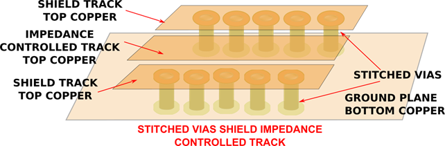
Placing a ground plane in the layer above the track and connecting it to the two copper lands and the bottom ground plane through more stitched vias turns the track into an internal microstrip.
As the vias and the ground planes shield the track, they define its impedance closely, and the track can carry high-speed signals with improved signal integrity.
The same plan works for isolating memory busses, shielding the analog sections, and any circuit handling sensors. Defining the edges of circuits with vias helps to prevent irregularities of shape from turning inadvertently into radiating antennas.
Improving EMI/EMC
Stitching vias all around the periphery of the PCB can help to improve its EMI/EMC characteristics. Designers place a copper plane about the same shape as the board, but size it to be smaller than the board outline by a few hundredths of an inch. Designers use a thumb rule known as the 3H rule, keeping any signal layer away by three times the dielectric thickness from the nearest ground plane. This method helps to keep spurious emissions in check.
This design rule causes the outer edges of the PCB to contain only the ground shapes while all other copper traces remain inside, away from the edges. By stitching the two ground planes on the top and bottom layers with multiple vias, the entire PCB forms a locked Faraday cage that drastically cuts down on all the harmonics that the FCC compliance requires.
Spacing the stitching vias depends on frequency they must suppress and the contract manufacturer’s capabilities. If the application requires very close spacing of vias that the contract manufacturer may have difficulty achieving, designers place a second row of ground vias within the first row.
Read About:
PCB Manufacturing and 5G
Can PCBs Carry High Voltage?
Conclusion
At PCB Trace Technologies Inc., we have experienced designers who use the simple ground via as an essential tool for enhancing current flow capabilities, improving thermal management, improving signal integrity, and improving the EMI/EMC performance of our customers’ boards, at practically no additional cost. As form factors of PCBs trends to ever-smaller outlines, our customers can rely on us to judiciously use vias to make a measurable different in the reliability of their products.
