Vias are plated-through holes connecting copper lands or traces on two different layers in multi-layered printed circuit boards or PCBs. PCB Trace Technologies Inc. offers several types of vias, including:
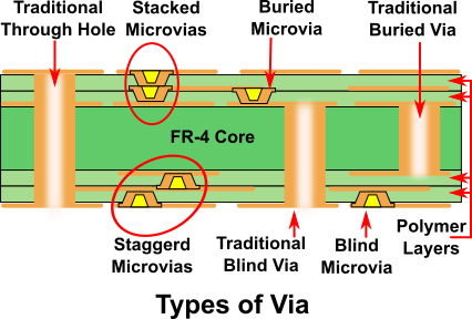
Through-Hole Vias: These are standard interconnecting holes that almost all printed circuit board use. Going all the through the thickness of the PCB, plated through-holes electrically connect copper lands and tracks from one layer to another. Fabricators typically use a metal drill bit for making the hole.
Blind Vias: Similar in construction to the through-hole via, a blind via begins on an external layer and ends on an internal layer. The layers it passes through, may or may not connect to the blind via.
Buried Vias: Again, similar in construction to the through-hole via, a buried via spans two internal layers within a multi-layered PCB, and may or may not connect to the other internal layers it passes through. A buried via is not visible on the external surfaces of a PCB.
Micro-Vias: Very useful for high-density interconnect or HDI boards, these tiny vias require lasers for drilling them, and they span just two adjacent layers. For spanning more than two layers, fabricators stagger or stack them. It is possible to create blind and buried micro-vias.

Although essential to effectively route a board, for high frequency design vias can add inductance to a circuit, just as traces do. Therefore, designers need to be wary of vias as they can affect the signal integrity of high-frequency nets.
With increasing pin-count of SMT components, and shrinking board size and thickness, designers face a tremendous challenge in routing high-density boards. This is where the via-in-pad technology helps them.
Via-In-Pad Technology
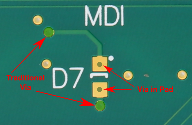
Via-in-pad or VIP technology essentially places a via within the metal pad of an SMT component. Traditionally, placing a via within the pad of an SMT component is fraught with the risk of creating a dry joint. During reflow, the via in an SMT pad is likely to wick the molten solder away from the pad to fill its hole, thereby starving the pad and the component surfaces of solder, leading to a dry joint.
However, fabricators have now started filling the via hole and plating the via pads. This prevents solder wicking, with the result that the quality of the VIP solder joint is comparable to a non-VIP joint. With the single weakness of VIPs thus taken care of, designers can make the most of the advantages of VIPs:
- Designers can now easily handle the breakout routing of SMT components that have a pin-pitch too narrow for employing traditional breakout routing using a pad and a separate via. Placing the via within the pad makes extra space available for routing traces.
- High speed designs require placing components close together, and designers use VIP for packing them densely.
- VIPs can shorten the connections to ground planes, and this is sometimes crucial to high-frequency designs.
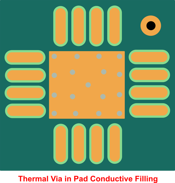
- High power components require thermal management to operate without failure. VIPs can help by transferring heat from the component to the other side of the PCB for connecting to a heat sink, thereby helping to remove the heat effectively.


Capping in VIP Technology
Compared to conventional vias, VIP technology takes more time and is more expensive during manufacturing. Conventional vias are not on pads, and therefore, a layer of solder mask will cover them. This prevents molten solder from wicking down the via hole during reflow.
In VIP technology, as the via is right on the pad, there is no solder mask covering. Therefore, fabricators must cap the via to prevent solder wicking. This requires an additional step in the manufacturing process.
As the via is on the pad, capping requires a material that solder can adhere to, as the pad will attach a component to it. However, covering the via with a cap poses another problem. Air trapped inside will outgas when the board heats up during reflow soldering, and may break the solder joint above it. This requires plugging or filling the via holes before capping them and adds another step in our manufacturing process.
Conductive and Non-Conductive Via Plugging
For non-conductive via plugging, PCB Trace Technologies Inc. uses an epoxy fill. Once the via formation is complete with copper plated walls, we use a squeegee and vacuum suction to draw the epoxy liquid into the via hole. We allow the epoxy to cure inside the hole. For conductive via plugging, we use an epoxy containing a conductive element, mostly silver. Conductive plugging adds to the via reliability and is better for thermal management.
After curing, the surface of the via needs planarizing, as we need to match the flatness of the via to that of the pad on the board. The conductive via is now a part of the pad.
Conclusion
PCB Trace Technologies Inc. uses VIP technology for its huge benefits. Using VIP technology results in boards with fewer layers, increase in channels for routing, better thermal management for components, and a better surface for soldering. Our vast experience in this field has led us to innovate and refine the technology for improving the quality of our HDI boards. VIP technology allows us to work with fine-pitch BGAs, assemble SMT devices closer than before, and improve the density of our assemblies, without any loss in functionality or reliability.
Read About:
What is Via Stitching and Why it is Useful?
