Check how easy it is to get a Full Trunkey quote in minutes

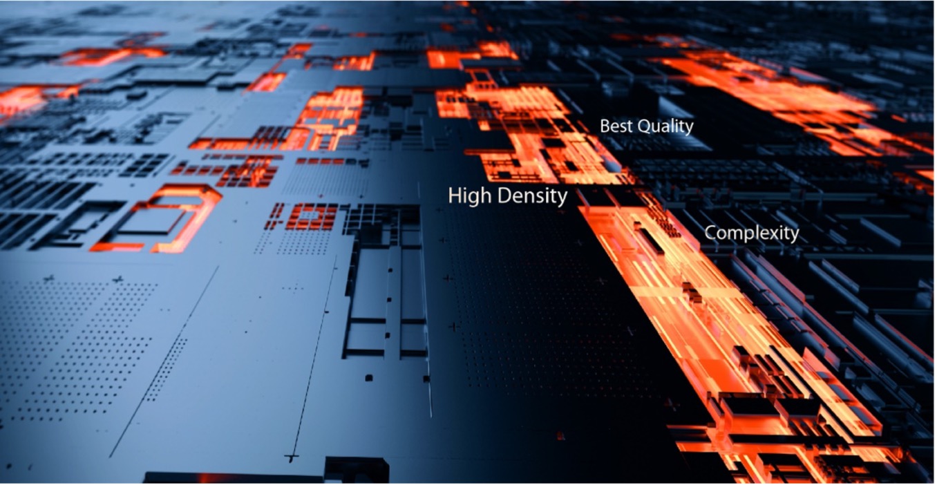
The hallmarks of today’s electronic systems are their high density, complexity and miniaturized size. To support such competitive list of features in a system, the packaging designs must meet all technical challenges arising as a result of these requirements. In fact, high quality packaging assists the system performance by facilitating thermal management, signal distribution, serviceability, manufacturing and power distribution. The PCB Trace Technologies Inc hardware engineering team includes SolidWorks and Autodesk certified engineers dedicated to overseeing the electronic packaging aspects of the projects. Our electronic packaging services incorporate reliability engineering and industrial design best practices to deliver the best quality packaging. Our expertise includes sheet metal and plastic enclosures, tooling, 3D printing, thermal management and design. The successful track record of our team in electronic packaging ranges from space-constrained wearable electronics design to thermally-critical power electronics modules and everything in-between.
Electronic Packaging Capabilities
- Packaging Design
- Sheet Metal and Plastic Enclosures
- Metal and Plastic Casting, Plastic 3D Printing
- Thermal Analysis
- Prototyping
- Ergonomics
- Concept and Graphics Generation
- Manufacturing Readiness
- Tooling Management
- Tooling Cost/Risk Analysis
- Vendor Evaluation and Selection
- Thermal Design
- Thermal Architecture
- Thermal Analysis using Computational Fluid Dynamics (CFD) Modeling
- Board-Level Thermal Design
- Heat sink Designs, Selection and Customization


Increased Production Panel Output
We can now ship 100 production panels of 18"x24" in 5-7 working days for 2 to 10 layer designs.
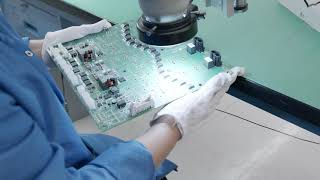
A glimpse into PCB Trace