Hole breakout is an important manufacturing defect in printed circuit boards (PCBs), particularly in multilayer, high-density interconnect (HDI), and fine-line PCB fabrication. During PCB manufacturing, drilled holes must be accurately positioned within their corresponding copper pads, lands, or internal-layer connections.
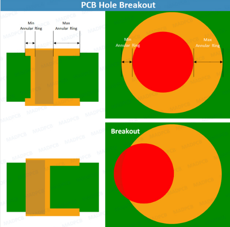
The copper area surrounding a drilled hole is known as the annular ring, and sufficient annular ring is necessary to maintain reliable electrical and mechanical connections. When a drilled hole is positioned too close to or beyond the edge of its intended copper pad, the copper surrounding the hole becomes insufficient or disappears completely at one or more locations. This condition is commonly referred to as hole breakout.
Hole breakout can occur because of drilling misregistration, dimensional movement of the PCB material, incorrect artwork compensation, drill-machine inaccuracies, tool runout, lamination movement, or insufficient design margins. Although a small amount of positional deviation may appear insignificant, it can have a major effect on electrical continuity, plating reliability, solderability, and long-term PCB performance. Therefore, adhering to high-quality manufacturing standards at PCB Trace Technologies Inc, controlling hole position, and maintaining adequate annular ring throughout the manufacturing process are essential requirements for producing reliable PCBs.
Understanding Hole Breakout
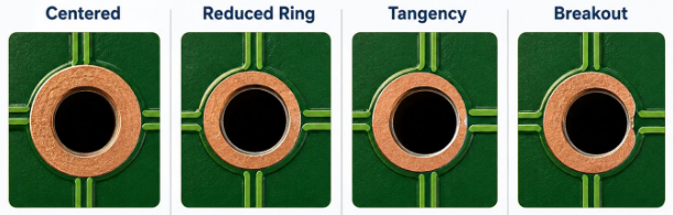
In a conventional PCB, a drilled hole is normally located approximately at the center of a copper pad. The pad is intentionally designed larger than the finished hole so that a continuous ring of copper remains around the hole after drilling. This copper ring provides the connection between the plated hole and the copper land or internal-layer circuit. When the hole shifts from its intended position, the available copper ring becomes smaller on one side and larger on the opposite side.
If the positional shift becomes sufficiently large, the drill may approach the edge of the pad and remove part of the copper land. This condition is called partial hole breakout. If the hole extends completely beyond the copper land at a particular layer, complete breakout may occur. The severity of breakout depends on the amount of positional displacement, the pad diameter, the finished hole diameter, the PCB layer construction, and the applicable design and manufacturing requirements.
Types of Hole Breakout
- Partial hole breakout occurs when a portion of the drilled hole extends beyond the edge of the copper pad while some copper remains around the hole. In this condition, the connection may still be electrically functional, but the reduced annular ring can create a reliability concern.
- Complete breakout occurs when the hole extends sufficiently beyond the intended copper feature that the required copper connection is no longer maintained. This condition is generally more serious because it can result in an open circuit or an unreliable plated connection.
- Internal-layer breakout, which occurs when a through-hole or via is not adequately registered with an internal copper pad. Since the internal layers cannot be visually inspected after lamination, this type of breakout can be difficult to identify without specialized inspection methods such as X-ray inspection or microsection analysis.
- External-layer breakout occurs on the outer surface of the PCB, where the drilled hole does not remain sufficiently centered within the surface pad. This may be easier to detect visually or through automated optical inspection, depending on the structure and surface finish.
Causes of Hole Breakout
One of the most common causes of hole breakout is drill-to-pad misregistration. The drill machine must position each hole according to the coordinates contained in the manufacturing data. Any deviation between the programmed drill location and the actual copper pad position can reduce the annular ring. The deviation can originate from machine accuracy, panel movement, tooling errors, or incorrect coordinate transformation.
Another important cause is dimensional movement of the PCB material. Laminates and copper layers can expand or contract as a result of temperature and moisture changes. During multilayer PCB manufacturing, materials are exposed to processes involving heating, pressing, cooling, and chemical treatment. These conditions can cause dimensional changes in the X and Y directions. If the dimensional movement is not properly compensated during manufacturing-data preparation, the drilled holes may no longer align accurately with the copper features.
Lamination movement is particularly important for multilayer PCBs. During lamination, heat and pressure are applied to bond cores, prepregs, and copper foils into a single structure. Resin flow, material expansion, copper distribution, press conditions, and cooling behavior can influence the final dimensions of the panel. As a result, the position of internal-layer features after lamination may differ slightly from their original positions. Drill data must therefore be appropriately compensated to account for expected dimensional movement.
Drill bit runout and mechanical condition can also contribute to hole-position errors. Drill bits rotate at very high speeds, and worn, damaged, improperly installed, or unsuitable tools can produce inaccurate holes. Excessive spindle runout, vibration, poor machine calibration, or improper panel support can cause the actual hole location to deviate from the programmed location. Tool wear can additionally affect hole quality and dimensional accuracy.
Hole Breakout During Multilayer PCB Manufacturing:
Multilayer PCBs present greater challenges because the drill must align with copper features located on several internal layers. A through-hole may pass through many dielectric and copper layers, and the position of the hole must remain compatible with the corresponding pads or lands on each relevant layer. Even if the outer surface appears correctly aligned, the hole may be slightly displaced relative to one or more internal layers.
This problem becomes more significant as the number of layers increases. Each manufacturing stage can introduce a small dimensional variation, and these variations can accumulate. Inner-layer imaging, etching, lamination, drilling, and subsequent plating must therefore be coordinated carefully. Manufacturers use registration targets, tooling systems, dimensional compensation, and inspection techniques to maintain alignment throughout the complete manufacturing process.
- Hole Breakout in HDI and Microvia PCBs
HDI PCBs require particularly strict registration control because their structures use smaller pads, smaller vias, finer traces, and tighter spacing. Microvias are commonly created using laser drilling, and the laser must be accurately positioned relative to the copper landing pad beneath the dielectric layer. If the microvia is displaced too far from the intended pad, insufficient copper may remain around the via.
Sequential buildup processes introduce additional registration challenges because each new dielectric and copper layer must align accurately with the previously fabricated structure. Any registration error can accumulate through successive buildup cycles. Consequently, HDI manufacturers use specialized imaging, laser drilling, registration, and inspection systems to maintain the required accuracy.
Effects of Hole Breakout on PCB Performance
The effect of hole breakout depends on its location, severity, and the electrical function of the affected feature. A minor reduction in annular ring may not immediately cause an electrical failure, but it can reduce the mechanical robustness of the connection. A severe breakout can produce an open circuit or an unreliable connection between the plated hole and the copper circuitry.
Hole breakout can also affect plated-through-hole reliability. During PCB operation, the board may experience thermal cycling, mechanical stress, and temperature changes. If the copper connection around a hole is already reduced because of breakout, the remaining structure may have less mechanical strength and greater susceptibility to cracking or separation.
In high-reliability applications, registration defects can therefore become a long-term reliability concern even when the board passes an initial electrical test. This is why manufacturers must control registration throughout fabrication rather than relying only on final electrical testing.
Detection and Inspection Methods
Hole breakout can be detected using several electrical testing methods depending on the PCB construction and manufacturing requirements. Automated optical inspection (AOI) can be used to inspect accessible outer-layer features and verify the relationship between holes and pads in suitable structures. However, AOI cannot directly inspect all internal-layer relationships in a completed multilayer PCB.
X-ray inspection can provide information about internal-layer alignment because X-rays can reveal the position of drilled holes relative to internal copper pads. This makes X-ray inspection particularly useful for complex multilayer and HDI structures where internal registration cannot be visually inspected.
Microsection analysis is another important method for evaluating hole breakout. In this method, a representative section of the PCB is cut through the relevant hole, prepared by grinding and polishing, and examined under magnification. The microsection allows engineers to observe the hole wall, copper plating, annular ring, internal-layer connections, and potential breakout directly. Microsection analysis is widely used for process qualification, failure analysis, and verification of PCB construction quality.
Prevention of Hole Breakout
Preventing hole breakout requires control of the complete PCB manufacturing process rather than focusing only on the drilling operation. The first step is to establish appropriate pad and hole dimensions that provide sufficient registration tolerance. Manufacturing capabilities should be considered during PCB design so that the required annular ring can be maintained under realistic production conditions.
Accurate data preparation and scaling compensation are also essential. PCB manufacturers analyze expected dimensional movement and apply appropriate compensation to manufacturing data. The compensation must account for material type, panel size, copper distribution, lamination behavior, and manufacturing experience.
Proper lamination process control is equally important. Press temperature, pressure, heating rate, cooling rate, resin flow, and material construction can influence final panel dimensions. Maintaining consistent lamination conditions helps reduce unpredictable movement between layers.
Drilling equipment should also be regularly calibrated and maintained. Drill bits must be selected according to the material and hole requirements, and worn tools should be replaced at appropriate intervals. Spindle runout, machine positioning accuracy, tooling condition, and panel support should be monitored to ensure repeatable hole placement.
Read More: FR-4 vs. Rogers – Choosing the Right PCB Material for High-Frequency Applications
Conclusion
Hole breakout is a significant PCB manufacturing defect associated primarily with insufficient registration between drilled holes and copper pads. It is strongly influenced by annular-ring design, drilling accuracy, laminate dimensional stability, lamination movement, tooling, manufacturing-data compensation, and process control. As PCB designs become more compact and incorporate finer features, the available registration margin becomes smaller, making accurate layer alignment increasingly important.
Effective prevention requires cooperation between PCB design and manufacturing teams, such as those at PCB Trace Technologies Inc. Adequate pad dimensions and annular-ring margins should be established during design, while manufacturers must control material movement, lamination, drilling, tooling, and inspection processes. AOI, X-ray inspection, and microsection analysis provide valuable methods for detecting and evaluating breakout. By implementing accurate registration systems, appropriate dimensional compensation, machine calibration, and continuous process monitoring, PCB manufacturers can significantly reduce hole breakout and improve the electrical, mechanical, and long-term reliability of printed circuit boards.