Copper foil plays a critical role in PCB manufacturing, influencing everything from electrical conductivity to signal integrity. At PCB Trace Technologies Inc., we recognize that its properties directly impact the performance, reliability, and efficiency of electronic devices. With various types, thicknesses, and surface treatments available, selecting the right copper foil is essential to meet specific design requirements. In multilayer PCB manufacturing, copper foil must also be compatible with the core and prepreg materials and must maintain good adhesion during lamination.
As PCB designs become thinner, denser, and increasingly focused on high-speed and high-frequency applications, copper foil selection has become more than simply choosing a standard copper thickness. Manufacturers and designers must consider copper profile, surface roughness, dimensional stability, plating interaction, and signal-loss characteristics to achieve a reliable and manufacturable PCB.
Role of Copper Foil in Multilayer PCBs
Copper foil is one of the most essential materials in PCB manufacturing. It is typically made from high-purity copper and is bonded to the surface of a PCB substrate, such as fiberglass or resin. Copper foil is extremely thin, usually ranging from a few micrometers to a few millimeters in thickness, and it is used to create electrical circuits on the PCB.
The composition of PCB copper foil consists of copper metal, which is known for its excellent electrical conductivity. This allows electrical signals and power to flow efficiently between components on the PCB. Without copper foil, PCBs would not be able to perform their primary function of connecting and powering the electronic components.
Types of Copper Foil
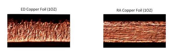
Copper foil used in PCB manufacturing can broadly be classified according to how it is produced. The two major categories are electrodeposited (ED) copper foil and rolled annealed (RA) copper foil.
ED Copper Foil is produced using an electroplating process, where copper ions are deposited onto a rotating cathode drum, which forms the foil. ED copper is widely used in conventional rigid multilayer PCBs because it can be manufactured economically in a wide range of thicknesses and is well suited to standard PCB fabrication processes.
RA Copper Foil is made by rolling copper into thin sheets and then annealing it to soften the material, giving it excellent flexibility and smoothness. It has a low surface roughness, which helps reduce signal loss, especially in high-frequency applications.
For conventional rigid multilayer PCB manufacturing, ED copper is commonly selected, while RA copper becomes more relevant when mechanical flexibility or specialized high-performance characteristics are required.
Copper Foil Thickness Selection
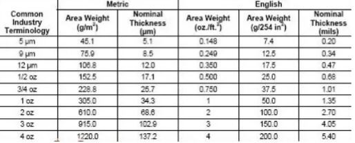
Copper thickness is one of the first parameters considered when selecting copper foil. Common PCB copper thicknesses range from very thin foils used for fine-line applications to much thicker copper used for high-current applications. The actual thickness may be specified in ounces per square foot or in micrometers.
As a general relationship, approximately 1 oz copper corresponds to about 35 µm of copper thickness. However, the final copper thickness after PCB fabrication can be greater than the starting foil thickness because additional copper may be deposited during plating.
Thin copper foil is advantageous for fine-line and high-density PCB manufacturing because it is easier to image and etch accurately. Thick copper provides greater current capacity and mechanical robustness but requires more careful control during imaging and etching because larger amounts of copper must be removed to create the desired circuit pattern.
Therefore, copper thickness should be selected based on the required current capacity, line width, spacing, impedance requirements, thermal requirements, and manufacturing capability.
Copper Foil Surface Treatment
Copper foil has two sides with different characteristics in many PCB constructions. One surface is designed to provide suitable adhesion to the dielectric material during lamination, while the opposite surface may have characteristics optimized for circuit processing.
Copper foil manufacturers may apply surface treatments or controlled roughening to improve adhesion between copper and the resin system. Proper adhesion is essential because copper must remain securely bonded to the dielectric throughout thermal cycling and subsequent PCB processing.
However, excessive copper roughness can become undesirable for high-frequency applications. A rough copper surface increases the effective electrical path length of high-frequency signals and can contribute to additional conductor loss. Therefore, the appropriate surface treatment depends on the intended electrical performance and frequency range of the PCB.
Copper Foil Roughness and High-Speed Signals
Copper surface roughness has become increasingly important with the growth of high-speed and high-frequency PCB applications. At high frequencies, current tends to concentrate near the conductor surface due to the skin effect. If the copper surface is significantly rough, the actual path followed by the high-frequency current becomes longer than it would be on an ideal smooth conductor.
This increased path length can contribute to greater insertion loss and signal attenuation. Consequently, high-speed PCB designs may use copper foils with controlled or low-profile surfaces to reduce conductor loss.
For high-frequency applications, copper foil selection should therefore consider not only nominal thickness but also roughness parameters and the compatibility of the foil with the laminate system and manufacturing process.
Copper Foil Adhesion
Strong adhesion between copper foil and the dielectric material is essential for multilayer PCB reliability. During lamination, the copper foil must bond effectively to the resin system. Poor adhesion can result in delamination, blistering, or separation during subsequent thermal processing.
Copper adhesion depends on several factors, including foil surface treatment, resin chemistry, lamination temperature, pressure, heating profile, and surface cleanliness. Manufacturers must ensure that the selected foil is compatible with the selected prepreg and core materials.
The surface must also be properly prepared before lamination. Contamination, oxidation, oil, dust, or improper handling can reduce adhesion and create reliability problems.
Copper Foil and Lamination
Copper foil selection has a direct relationship with multilayer lamination. During lamination, the copper foil, core, and prepreg materials are subjected to elevated temperature and pressure. The resin flows and bonds the layers together to create a stable multilayer structure.
The copper distribution across the panel can affect lamination behavior. Large differences in copper coverage between layers can contribute to variations in resin flow and dimensional movement. Copper balancing is therefore important when designing multilayer stack-ups.
Foil thickness can also influence the amount of resin required to fill the spaces around copper features. Heavy copper structures may require appropriate prepreg selection and resin content to ensure adequate filling without creating voids or excessive resin starvation.
Copper Distribution and Foil Selection
Copper distribution is an important consideration in multilayer PCB manufacturing. If one area of a layer contains a large copper plane while another area has very little copper, the panel may experience uneven thermal and mechanical behavior during processing.
Uneven copper distribution can contribute to panel warpage, dimensional movement, and registration problems. These effects can subsequently influence drilling accuracy and layer alignment.
For this reason, copper foil selection should not be considered independently of the PCB stack-up. The foil thickness and copper pattern on each layer should be evaluated together to maintain a balanced construction wherever practical.
Copper Foil for Controlled-Impedance PCBs
Copper thickness also influences controlled impedance. PCB impedance depends on conductor width, conductor thickness, dielectric thickness, and dielectric properties. Increasing copper thickness changes the conductor geometry and therefore affects the impedance of a transmission line.
When designing a controlled-impedance multilayer PCB, the selected copper foil thickness must be included in impedance calculations. The actual finished copper thickness after plating should also be considered for outer-layer controlled-impedance structures.
Manufacturing tolerances must be taken into account because variations in copper thickness and trace geometry can cause the final impedance to differ from the nominal design value. Therefore, copper foil selection and impedance control should be coordinated between PCB design and fabrication engineering.
Copper Foil and Etching
The copper foil thickness has a major effect on the etching process. During circuit formation, unwanted copper is chemically removed from the panel. Thicker copper requires greater etching capability and can produce more pronounced side etching.
Side etching causes the actual trace width at the bottom of the copper layer to differ from the width at the top. This effect becomes more significant as copper thickness increases relative to trace width. Consequently, heavy copper designs require careful artwork compensation and etching-process control.
For fine-line applications, thinner copper can provide better etching resolution. However, the manufacturing process must still maintain uniform copper thickness and avoid over-etching or under-etching.
Copper Foil Selection for Inner and Outer Layers
Inner and outer PCB layers may have different copper requirements. Inner signal layers commonly use thinner copper because they frequently contain fine traces and require controlled impedance. Outer layers may require thicker copper because they carry higher currents, contain component pads, or require additional plating.
When the outer layers undergo copper electroplating, the final copper thickness may increase significantly compared with the original foil thickness. This needs to be considered during design and manufacturing planning.
The difference between starting foil thickness and finished copper thickness should therefore be clearly understood. Manufacturing documentation should specify the appropriate requirements for both base copper and finished copper.
Copper Foil for High-Frequency PCBs
High-frequency PCB applications place additional requirements on copper foil. Besides thickness, manufacturers must consider surface roughness, treatment type, conductivity, and compatibility with low-loss dielectric materials.
Low-profile or very-low-profile copper foils can help reduce conductor loss in high-frequency circuits. These foils are increasingly important in applications such as high-speed networking, telecommunications, radar, automotive radar, and advanced computing systems.
However, reducing surface roughness can influence adhesion characteristics. Therefore, the foil treatment must provide an appropriate balance between low electrical loss and sufficient bonding strength.
Copper Foil for Thermal Management
Copper is also an important thermal conductor in PCB construction. Thicker copper layers and large copper planes can provide efficient pathways for spreading heat away from components.
In power electronics, copper foil thickness may therefore be selected partly according to thermal requirements. Copper planes can distribute heat across the PCB and transfer it toward thermal vias, heat sinks, metal-core structures, or other thermal-management components.
However, thermal requirements should be balanced against manufacturability. Very thick copper can increase board weight, etching difficulty, and cost. The optimum foil thickness is therefore determined by the complete electrical and thermal design.
Common Copper Foil Selection Problems
There are several problems can occur when copper foil is incorrectly selected. few of the most common ones:
- Thicker Copper Is Always Better: While thicker copper can handle more current, it’s not always necessary. Over-specifying copper thickness can unnecessarily increase costs without providing significant benefits.
- Thin Copper Is Only for Low-Power Designs: While thinner copper is used in low-power applications, it’s also critical for high-frequency designs where signal integrity is a priority.
- Copper Thickness Doesn’t Affect Design Software: Many PCB design tools require you to input copper thickness to calculate impedance and trace widths accurately. Ignoring this can lead to design errors.
Related: Reliability and Testing Strategies for Mission-Critical PCB Applications
Conclusion
Copper foil selection is a critical decision in multilayer PCB manufacturing because it affects electrical performance, thermal behavior, mechanical reliability, manufacturability, and cost. At PCB Trace Technologies Inc., the selection process considers copper thickness, foil type, surface roughness, surface treatment, adhesion characteristics, current requirements, signal frequency, lamination behavior, etching capability, and final copper thickness after plating.
For conventional multilayer PCBs, electrodeposited copper foil is widely used because of its compatibility with standard PCB manufacturing processes. Rolled annealed copper foil becomes more important where flexibility and specialized mechanical properties are required. Fine-line applications generally benefit from thinner copper, while power and high-current applications may require heavier copper. High-speed and high-frequency designs require additional attention to copper surface roughness and conductor-loss characteristics.
Ultimately, copper foil should be selected as part of the complete PCB stack-up and manufacturing process rather than as an isolated material choice. Proper coordination between PCB designers, material suppliers, and manufacturing engineers helps ensure that the selected copper foil provides the required electrical and mechanical performance while remaining compatible with imaging, etching, lamination, drilling, plating, and inspection processes.