Check how easy it is to get a Full Trunkey quote in minutes

To support our customer’s product requirements, PCB Trace Technologies Inc has developed a full array of Value Analysis and Value Engineering (VAVE) services aimed at balancing the design features, functionalities and associated cost. The VAVE is a continuous process that spans over the whole product management life cycle, from concept to post-production reviews. PCB Trace Technologies Inc. specializes in all aspects of VAVE from component engineering to product tear-down. Our optimized designs are geared toward being better in cost, profitability and efficiency.
Value Analysis and Value Engineering Capabilities
- Cost Reduction Analysis
- Bill of material analysis
- Electrical analysis
- Mechanical analysis
- Fabrication and assembly analysis
- Component Engineering
- Approved vendor list (AVL) expansion
- Cross vendor bill of material analysis
- Spend leverage analysis
- Restriction of hazardous materials / Waste electrical and electronic equipment (RoHS/WEEE)
- Obsolescence resolution
- Life cycle and risk analysis
- Service life and product longevity analysis
- Product Tear-Down
- Manufacturing assembly analysis
- Boothroyd Dewhurst techniques
- Competitive comparisons


Increased Production Panel Output
We can now ship 100 production panels of 18"x24" in 5-7 working days for 2 to 10 layer designs.
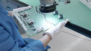
A glimpse into PCB Trace