Electronic devices nowadays offer higher functionality in increasingly smaller sizes. They do this by using larger numbers of small size components with higher PCB densities. Surface Mount Technology or SMT offers very small components, and High-Density Interconnect or HDI technology provides the high density for PCBs.
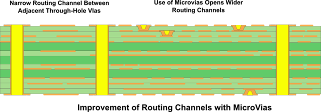
PCB Trace Technologies Inc. makes PCBs with HDI technology for creating very thin trace width/spacing. We do this by using the modified Semi-Additive Process or mSAP. We also use microvias as these play a critical role in increasing the routing density of our HDI boards—use of microvias opens wider routing channels.

With mSAP we can create traces down to 3 mil (0.075 mm) width. Using microvias allows us to use wider routing channels, thereby adding more traces than we could in between regular adjacent through-hole vias.
Although we can drill via holes of diameter 6 mil (0.15 mm) with mechanical drill bits, the tooling cost increases significantly as the thin drill-bits snap very easily, and need frequent replacement. With laser drilling we have overcome this problem, while at the same time we can drill via holes with diameter lower than 6 mil.
Drilling with Laser Via Technology
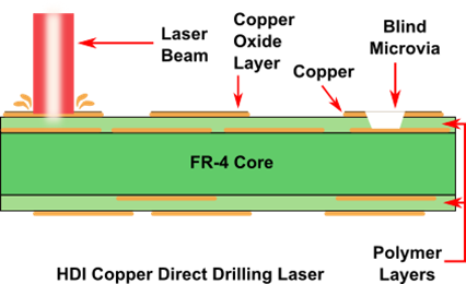
Today, laser via technology is a popular method for drilling small via holes, also known as microvia holes. We use infrared and ultraviolet wavelength lasers for drilling in HDI PCBs. For drilling, we program the laser beam for fluence size and energy. Low-fluence beams can drill through organic material but leaves metals undamaged. To cut through metal and glass, we use high-fluence beams. While low-fluence beams require beams of 4-14 mil (0.1-0.35 mm) diameter, high-fluence beams require beams of about 1 mil (0.02 mm) diameter.

Advantages of Laser Drilling
Compared to mechanical drilling, creating microvias with laser drilling technology offers several advances crucial to HDI PCBs. Some of these are:
Non-contact technique—Laser drilling technology is completely non-contact. As the drilling bit is a beam of light, there is no physical contact between the drill bit and the workpiece or PCB, and therefore, the drill-bit does not wear out. Moreover, no contact means the printed circuit board remains free from contamination.
Small diameter vias—Laser drilling produces very small vias with diameters ranging from 3-6 mil (0.075-0.15 mm) diameter, which the traditional mechanical drill bit cannot achieve. This small diameter microvias are crucial to the creating the high density of an HDI board, as it significantly increases the routing density, thereby contributing to the huge success of the HDI boards.
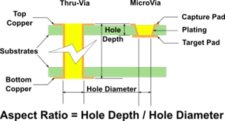
Better aspect ratio—Laser drilling allows achieving better aspect ratios for vias. This ratio, representing the hole depth to hole diameter of a via, can range from 10:1 to 8:1 for standard mechanically drilled vias. For a 62 mil (1.6 mm) thick PCB, this ratio represents a hole diameter ranging from 6-8 mil, a maximum limit for the mechanical drilling process. Reaching 6 mil hole diameter with mechanical drilling is very inefficient and expensive for most PCB manufacturers. With laser drilling, microvias conforming to IPC can have a maximum aspect ratio of 1:1, for a hole where the depth does not exceed 10 mil (0.25 mm). This is because the microvia has a different profile compared to a regular via, resulting in a different aspect ratio.

Higher throughput—When the PCB has numerous densely located vias, mechanical drilling can be very slow. On the other hand, laser drilling is significantly faster, even for drilling densely placed vias on a multilayer board. Moreover, as time passes, the extra costs from frequently replacing broken drill bits adds up and mechanical drilling can become far more expensive compared to laser drilling.
Higher Precision—For mechanical drilling, typical PTH tolerance is ±4 mil, and NPTH tolerance is ±3 mil. This tolerance is much lower for laser drilling, with ±3 mil as the maximum. This allows formation of blind, buried, and stacked vias when manufacturing HDI boards.
As a focused laser beam can have only a limited depth before it loses focus, it can produce reliable holes repeatedly only if the hole is also of limited depth. If only a single lens focuses the beam, it limits the depth of focus, and the laser cannot drill deep holes. A larger number of lenses forming a collimated laser beam can form longer focused laser beams and hence drill deeper holes. However, as the diameter of the hole is small, the beam experiences Fresnel diffraction, reducing the intensity of the beam as the hole becomes deeper.
Types of Laser Drilling
For drilling microvias, PCB manufacturers use many variations of lasers. Most popular in the industry are five laser combination systems:
- CO2/TCO2 Laser
- Yag/CO2 Laser
- CO2 Laser
- UV/Tag Laser
- UV/Excimer Laser
Different laser combinations are necessary as PCB manufacturers use several dielectric materials like resin (liquid or dry film), reinforced prepreg, and RCC. Depending on the dielectric material, and using one of the five laser systems above, PCB manufacturers successfully make reliable microvia holes.
For infrared wavelengths, PCB Trace Technologies Inc. uses CO2 lasers, as these are economical and readily available. We use the CO2 laser primarily for laminates without glass fibers, such as laminates reinforced with aramid fibers, flexible polyimide, and resin-coated copper or RCC foils. For lazing through glass fibers, we prefer to use the Transversely Excited Atmospheric or TEA CO2 laser with higher peak power.
Conclusion Microvias formed with laser drilling is crucial to the high densities offered by HDI boards. It would not be possible to achieve very high densities with thin traces and smaller spacing alone. Microvias, with their small diameters, combined with staggering and stacking, significantly widens the routing channels for achieving the incredibly high routing densities in PCB Trace Technologies Inc. HDI boards.
