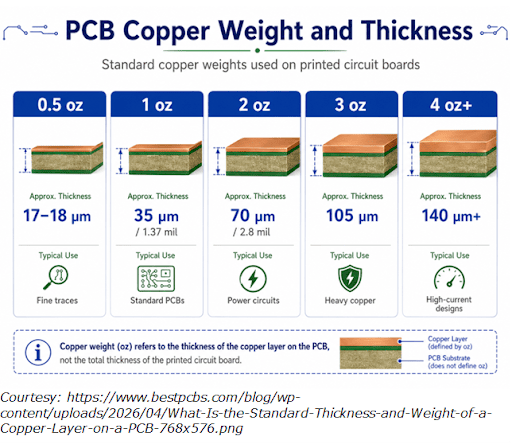
At PCB Trace we manufacture various types of Printed Circuit Boards (PCBs) with copper weight selected according to the application of the board. Designers often require a specific copper thickness when accommodating the current requirement of their design. We offer a variety of copper weights to help you meet your design requirements.
Definition of PCB Copper Weight
This is weight of the copper foil on a PCB, commonly termed as ounces of copper per square foot area. The parameter represents the overall thickness of the copper foil on the layer.
PCB Trace offers the following copper weights (pre-plating) for the PCBs we fabricate. We measure the weight in oz/ft2. Designers can select the appropriate copper weight to fit their design needs:
0.5 oz Copper – This weight represents a copper thickness of ~17.5 µm or 0.7 mils and is available for internal layers for non-standard construction of PCBs. This also forms the standard starting copper weight for PCBs that have the 1 oz finished copper weight.
1.0 oz Copper − This weight represents a copper thickness of ~35 µm or 1.4 mils and is the standard construction product for 1 oz and 2 oz finished copper weight PCBs. For external layers, this is also the starting copper weight for PCBs with 2 oz finished copper weight.
2 oz Copper – This weight represents a copper thickness of ~70 µm or 2.8 mils and is the standard copper thickness for the internal layers on a PCB with 3 oz finished copper weight.
3 oz Copper – This weight represents a copper thickness of ~105 um or 4.2 mils and is the standard copper thickness for boards requiring very high current capacity and durability.
Non-Standard – PCB Trace also offers a selection of additional copper weights starting from 0.25 oz/ft2 to 6 oz/ft2.
Why Does PCB Copper Weight Matters?
Selection of copper weight directly influences the board’s ability to carry the required electric current, manage the heat build-up, and ensure overall reliability. The three most common options, 1 oz, 2 oz, and 3 oz copper, each present distinct and unique advantages and compromises related to current capacity, temperature rise, voltage drop, impedance matching, mechanical strength, cost, and manufacturability.
Basics of Copper Weight
The ounce (oz) unit is chosen as 1 oz of copper by weight, when spread over one square foot of PCB is approximately 35 µm or 1.4 mil thick.
As stated above, the practical application for copper weights are:
- 1 oz ≈ 35 µm or 1.4 mil copper thickness
- 2 oz ≈ 70 µm or 2.8 mil copper thickness
- 3 oz ≈ 105 µm or 4.2 mil copper thickness
The above are the base copper weights. Therefore, the finished copper thickness may be different, especially after the plating process.
Where does Copper Weight Apply?
In general, copper weight applies on all the layers of a PCB. While it is common for some layers to have heavier copper than on others, design rule practices call for the same copper weight to be used on the mirrored opposite layer in the stackup.
For instance, in a 4-layer board, layers 1 and 4 can be 2 oz, while layers 2 and 3 can be 1 oz. This arrangement offers a balanced stack and reduces the chance of the board to twist or bow when it is heated during use or assembly.
Therefore, if the board has a top copper layer with a finished copper weight of 3 oz, then the bottom copper layer should also have a finished copper weight of 3 oz.
In multilayer boards, the top and bottom layers are designed to carry high currents, while the inner layers mostly carry signals and low currents. Therefore, it is customary to have 1 oz copper in the innermost layers, 2 oz copper in the intermediate layers for traces and power planes, and 3 oz copper in the outermost layers carrying heavy-current traces.
Necessity for 2 oz and 3 oz copper
Although 1 oz is the industry standard copper weight for PCBs, 1 oz copper has its limitations, which are overcome by using 2 oz and 3 oz copper. The advantages are:
Higher Capacity to Carry Current
Thicker copper has the ability to carry higher amounts of current without failing or overheating. Typically, the current-carrying capacity of copper traces depend on their cross-sectional area. Therefore, a 2 oz trace can carry twice the amount of current that a 1 oz trace of the same width can carry. Similarly, a 3 oz trace of the same width can carry almost three times the current as compared to the 1 oz trace.
Better Thermal Management
Copper is a very good conductor of heat and increasing its thickness improves its heat carrying capacity even further, allowing for better thermal distribution across the board. Using 2 oz or 3 oz copper reduces the risk of hot spots that over time, can degrade the board performance and even damage components.
Enhanced Mechanical Strength
2 oz or 3 oz copper layers, being thicker than 1 oz, add to the structural integrity of the PCB. This makes the board more resistant to mechanical stress and vibration. Therefore, a 2 oz or 3 oz copper PCB is less likely to delaminate or develop cracks compared to the thinner 1 oz board when subjected to the same physical stress.
Reduced Voltage Drop
When traces carry high currents, the resistance of the trace leads to voltage drop along the length of the trace. This often leads to issues like performance drop and inefficiency. Using thicker copper increases the cross-sectional area leading to lower resistance of the traces, minimizing voltage drops. This ensures stable power delivery to high-current components.
For instance, the resistance of a 2 oz trace is approximately halved compared to that of a 1 oz trace of the same width. A 3 oz trace of the same width offers an even lower resistance.
Where to use
1 oz Copper
Standard low-cost choice for general-purpose PCBs
Widely available fabrication capability
Supports fine traces/spaces, suitable for dense routing
Typical applications involve digital logic boards, microcontrollers, low-power analog circuits, consumer electronics
Limitations include higher resistance and voltage drop at higher currents leading to temperature rise.
2 oz Copper
Practically a middle ground between signal routing and power handling
Less suitable for fine-pitch and high-density routing
Roughly double the current capacity compared to 1 oz for the same trace width
Lower trace resistance and voltage drop, better heat management
Can use narrower power traces compared to 1 oz for the same current
Requires wider trace/space rules due to etching effects
Higher PCB cost
Typical applications involve moderate power path PCBs
3 oz copper
Is the entry point for heavy-copper high-current PCB manufacturing
Substantially higher current and power handling capacity compared to 1 oz and 2 oz PCBs
Improved mechanical strength and durability in adverse environments
Not suitable for dense routing
Not suitable for controlled-impedance designs
Requires wider traces/spaces
Higher PCB cost, fabrication cost, and longer lead times
Typical applications involve high-current applications and high-power applications.
Comparison of 1 oz, 2 oz, and 3 oz Copper
| Parameter | 1 oz Copper | 2 oz Copper | 3 oz Copper |
| Thickness (µm) | 35 | 70 | 105 |
| Use Cases | General purpose logic and low-power circuits | Mid-power and mixed signal-power boards | High-current, high-power circuit boards |
| Current Handling | Low currents | Moderate currents | Heavy currents |
| Trace Resistance | Highest | Moderately low | Lowest |
| Voltage Drop | Highest | Moderate | Lowest |
| Routing Density | Highest | Moderate | Constrained |
| Manufacturing Cost | Lowest | Moderate | Highest |
| Manufacturing Complexity | Standard | Higher | Heavy-copper process |
Conclusion
Although for most designs, 1 oz is a suitable and sufficient choice, when it comes to handling higher currents, we, at PCB Trace, suggest using 2 oz copper. For genuinely high-power applications, we prescribe the 3 oz copper option.
FAQs
How is PCB copper thickness specified?
PCB copper thickness is specified in copper weight in ounces over 1 square foot.
What are the standard copper thicknesses used in the industry?
For low-power/low-current requirement – 1 oz
For medium-power/medium-current requirement – 2 oz
For high-power/high-current requirements – 3 oz and more.
Can you use 3 oz copper in inner layers of a PCB
In general, the inner layers of a PCB handle only low and medium currents such as for signals and interconnections, for which, 1 oz is more suitable. 3 oz copper is for handling high currents, and is used only in the outermost layers of a PCB.
Why does thicker copper offer lower resistance?
The resistance of a conductor depends inversely on its cross-section. For the same trace width, thicker copper has a higher cross-section, hence its resistance is lower.
Why does thicker copper not allow close spacing?
Etching thicker copper is more difficult, as the etching produces uneven spacing. Therefore, thicker copper requires more spacing.
How to know what copper thickness is required?
The easiest way is to study the current requirement. You can also use a PCB trace calculator, Copper weight calculator and Copper thickness calculator included in most PCB design software packages.