The rapid growth of electronic products has made the productivity and quality requirements of manufacturing electronic products rather complicated and strict. While end consumers demand higher quality and stability from electronic products during their entire life cycle, product engineering teams require that the design of PCBs or printed circuit boards use small and precisely placed electronic components. Eminent PCB manufacturers like PCB Trace Technologies Inc. know that for effective mass production of electronic products, the PCBA or printed circuit board assembly requires SMT or surface mount technology.
The finished product quality and yield performance require an effective adoption of SMT, especially while handling tiny component package sizes like the 0201. A generic PCBA production flow has essential equipment that includes stencil printers, placement machines, and reflow ovens. To prevent failures, manufacturers use several failure-prevention processes in their production lines. These include solder paste inspection (SPI), automated optical inspection (AOI), and in-circuit testing (ICT).
Smart Manufacturing
At present, failure prevention processes are mostly reactive, that is, based on occurring defects. This method creates finite production waste products and requires additional efforts to recover them. Therefore, manufacturers attempt to transform these processes to make them proactive and align them automatically with their objective of smart manufacturing. To achieve this, domain experts set the parameter setting of the PCBA machines. That makes the entire process highly reliant on the expert knowledge of the domain experts, which cannot be effectively transferred to others. Moreover, calculations for the yield loss of the PCBA process use the investigations from the existing inspection process, while not considering its effect on the parameter settings of the machine. That makes it difficult to optimize the process performance, while the yield performance depends on the expertise of domain experts.
Improved Smart Manufacturing
To overcome the challenges in the existing PCBA process mentioned above, manufacturers are resorting to another type of smart manufacturing. This depends on a technology-driven method of automating the manufacturing operations to improve their performance with data analytics. This type of smart manufacturing involves six pillars, namely:
- Data collection
- Predictive Engineering
- Resource sharing and networking
- Manufacturing technology and processes
- Sustainability
- Materials
Following the smart manufacturing pillars mentioned above imbibe a higher intelligence to the entire PCBA process, making it independent of human intervention. Manufacturers can formulate proactive strategies while managing their production processes. This ultimately results in the PCBA process becoming more intelligent and automated.
Artificial Intelligence in PCB Manufacturing
The advent of ML or machine learning and AI or artificial intelligence has brought more challenges for engineers designing and producing PCBs. The rapid growth and demand for AI are significantly affecting the PCB industry, evolving production quality and throughput.
This is due to AI being capable of solving PCB quality issues that were not possible earlier. For instance, AI can already identify known defects, such as soldering problems and missing components. But it can also identify weaknesses that were not seen earlier.
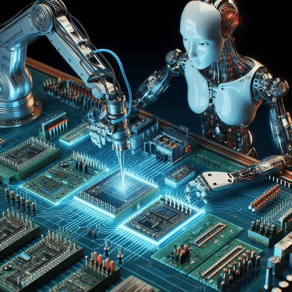
The system typically uses computer vision technology along with machine learning capabilities. It captures images from several angles and uses pattern recognition algorithms to compare with known defects, reporting them to operators for further rework. There are primarily three areas where PCBA uses AI:
AI-Based Optical Inspection
During PCB production, optical inspection is one way of identifying or detecting defective products. This is a vital link to improve the quality of boards and to reduce production costs. However, manual optical inspection is a time-consuming and tedious process, often prone to human error. On the other hand, AI-based optical inspection can achieve higher speeds and accuracy in defect identification using deep learning algorithms.
AI-Assisted Soldering Machines
AI-assisted soldering machines use nozzles to solder tiny SMT parts to the PCB. These are highly productive, especially for fine-pitch ICs.
AI-Assisted Predictive Maintenance
The PCB fabrication process has many smart sensors that capture numerous data from different machines. Computers analyze the captured data to identify error-prone areas in the flow process. Such predictive maintenance can reduce the downtimes in the assembly line, thereby avoiding impending losses.
Considerations for AI Integration
To achieve the full benefits of Artificial Intelligence in PCB assembly, it is necessary to consider some key factors:
- Data accuracy, as it is necessary to use the data further during analysis and strategy planning. Automation software requires accurate data inputs for proper fault detection.
- Adequate data collection from the production line, as this improves the precision of AI-based analysis and output.
- Expertise in AI for PCB manufacturing, as this is critical to achieving the best results. Operators can feel overwhelmed by large quantities of captured data if they cannot understand it properly.
- Research and continuous improvement in AI for PCB manufacturing, as this helps to achieve the best results. The involvement of AI, ML, and DL or deep learning in PCB manufacturing leads to minimal human intervention in the production process, specifically leading to a reduction in human errors.
AI, Industry 4.0, and PCB Assembly
AI is presenting tremendous opportunities in PCB manufacturing and assembly. Starting from PCB design, where automated routing and design of boards are outperforming manual methods, improving design time and quality.
For instance, AI is improving the placement of components in PCB design, helping to streamline production processes, and improving outcomes in many ways.
Moving towards Industry 4.0, AI is helping automation systems communicate with operators and with each other in real time. This brings several benefits to manufacturing, including a reduction in scrap, better performance, and efficient management of inventory, assets, and supply chains.
With the market embracing Industry 4.0, the smart factory of the future, the introduction of AI in PCB assembly is especially critical. For instance, it is now possible to embed AI in the precision placement tool, helping to decide the proper placement of each component, thereby improving its performance while reducing the assembly time.
PCBs are getting progressively smaller, keeping step with the reducing form factor of devices, and AI is allowing manufacturers to achieve a higher degree of accuracy while their placement tool places components in a compact and densely packed board.
Another area where AI is proving its worth during PCB assembly is in inspections. It saves both time and money when locating a fault.
However, in all this discussion, the main component is data. Artificial Intelligence in PCB assembly process can only succeed when the data is of high quality. For instance, in PCB assembly, AOI or automated optical inspection has a crucial role of defect classification. Typically, AOI machines transmit images to a verification station, where a human operator must classify them as false alarms or true defects. However, the human element is prone to errors and the classification can easily become doubtful.
However, once the AI solution has learned from the decisions of a human operator, it can autonomously make the classifications distinctly and with consistent accuracy. The AI system is dependent only on accurate data patterns and learns the correct method of classification through algorithmic behavior over time.
Future of AI and PCB Assembly
At present, the situation in current technologies related to PCB assembly classifies AI as weak or narrow. This is because its design is targeted to perform only specific tasks such as placing components on the board, looking for solder defects, or searching for missing components.
However, for developers, the long-term objective is to create a strong or general AI. While narrow AI can outperform humans at specific tasks, a strong AI could take over much of the cognitive tasks of humans.
Conclusion
With the increasing involvement of Artificial Intelligence in PCB assembly and manufacturing practices, it will likely become mission-critical to the success of projects. Moving forward, the application of AI will surely have a positive impact on the speed of operational processes, including dependability and trust. At PCB Trace Technologies Inc., we expect the technology to take the PCB manufacturing industry to a wholly new level.
